
1 Mbit nvSRAM Specification Sheet


PRELIMINARY
CY14B101Q1
CY14B101Q2
CY14B101Q3
Document #: 001-50091 Rev. *A Page 11 of 22
nvSRAM Special Instructions
CY14B101Q1/CY14B101Q2/CY14B101Q3 provides four
special instructions which enables access to four nvSRAM
specific functions: STORE, RECALL, ASDISB, and ASENB.
Tab l e 8 lists these instructions.
Software STORE
When a STORE instruction is executed, nvSRAM performs a
Software STORE operation. The STORE operation is issued
irrespective of whether a write has taken place since last STORE
or RECALL operation.
To issue this instruction, the device must be write enabled (WEN
bit = ‘1’). The instruction is performed by transmitting the STORE
opcode on the SI pin following the falling edge of CS
. The WEN
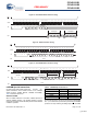
Figure 12. Burst Mode Read Instruction Timing
Figure 13. Write Instruction Timing
Figure 14. Burst Mode Write Instruction Timing
CS
SCK
SO
LSB
SI
Op-Code
17-bit Address
MSB
LSB
~
~
~
~
~
~
01 2 3 456 7
0
765432
1
20 21 22 23
01234567 01234567
~
~
0
7
0000 00
11 0 0 00 00 0
A16
A3 A2 A1 A0
D0
D1
D2D3
D4
D5
D6
D7
Data Byte 1
Data Byte N
MSB
LSB
MSB
D0
D1
D2D3
D4
D5
D6
D7
D0D7
~
~
CS
SCK
SO
01234 5
6
7
0
765432
1
2021222301234567
MSB LSB
Data
D0D1
D2
D3
D4
D5D6D7
SI
~
~
Op-Code
00 00001
000 0
0
0
0
0
A16 A3
A1A2
A0
17-bit Address
MSB LSB
HI-Z
~
~
CS
SCK
SO
MSB
LSB
SI
Op-Code
17-bit Address
MSB
LSB
~
~
~
~
01 234567
0
76 5 432
1
20 21
22 23
01 234567 01 234567
~
~
0
7
0 00000
100000000
A16
A3 A2 A1 A0
HI-Z
Data Byte 1
Data Byte N
D0
D1
D2D3
D4
D5
D6
D7
D0
D1
D2D3
D4
D5
D6
D7
D0D7
Table 8. nvSRAM Special Instructions
Function Name Opcode Operation
STORE 0011 1100 Software STORE
RECALL 0110 0000 Software RECALL
ASENB 0101 1001 AutoStore Enable
ASDISB 0001 1001 AutoStore Disable
[+] Feedback