
1 Mbit nvSRAM Specification Sheet


PRELIMINARY
CY14B101Q1
CY14B101Q2
CY14B101Q3
Document #: 001-50091 Rev. *A Page 14 of 22
AC Test Conditions
Input Pulse Levels.................................................... 0V to 3V
Input Rise and Fall Times (10% - 90%) ....................... <3 ns
Input and Output Timing Reference Levels.....................1.5V
Data Retention and Endurance
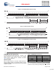
Parameter Description Min Unit
DATA
R
Data Retention 20 Years
NV
C
Nonvolatile STORE Operations 200 K
Capacitance
Parameter
[6]
Description Test Conditions Max Unit
C
IN
Input Capacitance T
A
= 25°C, f = 1MHz,
V
CC
= 3.0V
6pF
C
OUT
Output Pin Capacitance 8 pF
Thermal Resistance
Parameter
[6]
Description Test Conditions 8-SOIC 8-DFN Unit
Θ
JA
Thermal Resistance
(Junction to Ambient)
Test conditions follow standard test
methods and procedures for measuring
thermal impedance, per EIA / JESD51.
TBD TBD °C/W
Θ
JC
Thermal Resistance
(Junction to Case)
TBD TBD °C/W
Figure 20. AC Test Loads and Waveforms
3.0V
OUTPUT
5 pF
R1
R2
789Ω
3.0V
OUTPUT
30 pF
R1
R2
789Ω
577Ω
577Ω
Note
6. These parameters are guaranteed by design and are not tested.
[+] Feedback