
1 Mbit nvSRAM Specification Sheet

PRELIMINARY
CY14B101Q1
CY14B101Q2
CY14B101Q3
Document #: 001-50091 Rev. *A Page 2 of 22
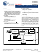
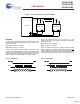
Pinouts
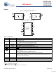
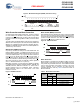
Figure 1. Pin Diagram - 8-Pin DFN
[1, 2, 3]
Figure 2. Pin Diagram - 16-Pin SOIC
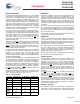
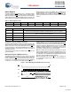
Table 1. Pin Definitions
Pin Name I/O Type Description
CS
Input Chip Select. Activates the device when pulled LOW. Driving this pin high puts the device in low
power standby mode.
SCK Input Serial Clock. Runs at speeds up to max 40 MHz. All inputs are latched at the rising edge of this
clock. Outputs are driven at the falling edge of the clock.
SI Input Serial Input. Pin for input of all SPI instructions and data.
SO Output Serial Output. Pin for output of data through SPI.
WP
Input Write Protect. Implements hardware write protection in SPI.
HOLD
Input HOLD Pin. Suspends Serial Operation.
HSB
Input/Output Hardware STORE Busy: A weak internal pull up keeps this pin pulled high. If not used, this pin is
left as No Connect.
Output: Indicates busy status of nvSRAM when LOW.
Input: Hardware STORE implemented by pulling this pin LOW externally.
V
CAP
Power Supply AutoStore Capacitor. Supplies power to the nvSRAM during power loss to STORE data from the
SRAM to nonvolatile elements. If AutoStore is not needed, this pin must be left as No Connect. It
must never be connected to GND.
NC No Connect No Connect: This pin is not connected to the die.
GND Power Supply Ground
V
CC
Power Supply Power Supply (2.7 to 3.6V)
CY14B101Q2
Top View
not to scale
CS
SO
V
CAP
GND
V
CC
HOLD
SCK
SI
CY14B101Q1
Top Vi ew
not to scale
CS
SO
WP
GND
V
CC
HOLD
SCK
SI
NC
GND
WP
V
CAP
1
2
3
4
5
6
7
8
9
10
11
12
13
NC
16
15
14
V
CC
SO
SI
SCK
CS
HSB
NC
NC
NC
HOLD
NC
CY14B101Q3
Top V iew
not to scale
Notes
1. HSB
pin is not available in 8 DFN packages.
2. CY14B101Q1A part does not have WP
pin.
3. CY14B101Q2A part does not have V
CAP
pin and does not support AutoStore.
[+] Feedback