
1 Mbit nvSRAM Specification Sheet

PRELIMINARY
CY14B101Q1
CY14B101Q2
CY14B101Q3
Document #: 001-50091 Rev. *A Page 3 of 22
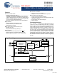
Device Operation
CY14B101Q1/CY14B101Q2/CY14B101Q3 is 1 Mbit nvSRAM
memory with a nonvolatile element in each memory cell. All the
reads and writes to nvSRAM happen to the SRAM which gives
nvSRAM the unique capability to handle infinite writes to the
memory. The data in SRAM is secured by a STORE sequence
which transfers the data in parallel to the nonvolatile Quantum
Trap cells. A small capacitor (V
CAP
) is used to AutoStore the
SRAM data in nonvolatile cells when power goes down providing
power down data security. The Quantum Trap nonvolatile
elements built in the reliable SONOS technology make nvSRAM
the ideal choice for secure data storage.
The 1 Mbit memory array is organized as 128K words x 8 bits.
The memory can be accessed through a standard SPI interface
that enables very high clock speeds upto 40 MHz with zero cycle
delay read and write cycles. This device supports SPI modes 0
and 3 (CPOL, CPHA = 0, 0 & 1, 1) and operates as SPI slave.
The device is enabled using the Chip Select pin (
CS
) and
accessed through Serial Input (SI), Serial Output (SO), and
Serial Clock (SCK) pins.
This device provides the feature for hardware and software write
protection through WP
pin and WRDI instruction respectively
along with mechanisms for block write protection (1/4, 1/2, or full
array) using BP0 and BP1 pins in the status register. Further, the
HOLD
pin can be used to suspend any serial communication
without resetting the serial sequence.
CY14B101Q1/CY14B101Q2/CY14B101Q3 uses the standard
SPI opcodes for memory access. In addition to the general SPI
instructions for read and write, it provides four special
instructions which enable access to four nvSRAM specific
functions: STORE, RECALL, AutoStore Disable (ASDISB), and
AutoStore Enable (ASENB).
The major benefit of nvSRAM SPI over serial EEPROMs is that
all reads and writes to nvSRAM are performed at the speed of
SPI bus with zero delay. Therefore, no wait time is required after
any of the memory accesses. The STORE and RECALL
operations need finite time to complete and all memory accesses
are inhibited during this time. While a STORE or RECALL
operation is in progress, the busy status of the device is indicated
by the Hardware STORE Busy (HSB
) pin and also reflected on
the RDY
bit of the Status Register.
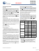
The Device is available in three different pin configurations that
enable the user to choose a part which fits in best in their appli-
cation
. The Feature summary is given in Table 2.
SRAM Write
All writes to nvSRAM are carried out on the SRAM and do not
use up any endurance cycles of the nonvolatile memory. This
enables user to perform infinite write operations. A Write cycle is
performed through the SPI WRITE instruction. The WRITE
instruction is issued through the SI pin of the nvSRAM and
consists of the WRITE opcode, three bytes of address, and one
byte of data. Write to nvSRAM is done at SPI bus speed with zero
cycle delay.
The device allows burst mode writes to be performed through
SPI. This enables write operations on consecutive addresses
without issuing a new WRITE instruction. When the last address
in memory is reached, the address rolls over to 0x0000 and the
device continues to write.
The SPI write cycle sequence is defined explicitly in the Memory
Access section of SPI Protocol Description.
SRAM Read
A read cycle is performed at the SPI bus speed and the data is
read out with zero cycle delay after the READ instruction is
performed. The READ instruction is issued through the SI pin of
the nvSRAM and consists of the READ opcode and 3 bytes of
address. The data is read out on the SO pin.
This device allows burst mode reads to be performed through
SPI. This enables reads on consecutive addresses without
issuing a new READ instruction. When the last address in
memory is reached in burst mode read, the address rolls over to
0x0000 and the device continues to read.
The SPI read cycle sequence is defined explicitly in the Memory
Access section of SPI Protocol Description.
STORE Operation
STORE operation transfers the data from the SRAM to the
nonvolatile Quantum Trap cells. The device stores data to the
nonvolatile cells using one of three STORE operations:
AutoStore, activated on device power down; Software STORE,
activated by a STORE instruction in the SPI; Hardware STORE,
activated by the HSB
. During the STORE cycle, an erase of the
previous nonvolatile data is first performed, followed by a
program of the nonvolatile elements. After a STORE cycle is
initiated, further input and output are disabled until the cycle is
completed.
The HSB signal or the RDY bit in the Status register can be
monitored by the system to detect if a STORE cycle is in
progress. The busy status of nvSRAM is indicated by HSB
being
pulled LOW or RDY
bit being set to ‘1’. To avoid unnecessary
nonvolatile STOREs, AutoStore and Hardware STORE opera-
tions are ignored unless at least one write operation has taken
place since the most recent STORE or RECALL cycle. Software
initiated STORE cycles are performed regardless of whether a
write operation has taken place.
AutoStore Operation
The AutoStore operation is a unique feature of nvSRAM which
automatically stores the SRAM data to QuantumTrap during
power down. This Store mechanism is implemented using a
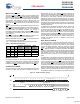
Table 2. Feature Summary
Feature CY14B101Q1 CY14B101Q2 CY14B101Q3
WP
Yes No Yes
V
CAP
No Yes Yes
HSB
No No Yes
AutoStore No Yes Yes
Power Up
RECALL
Yes Yes Ye s
Hardware
STORE
No No Yes
Software
STORE
Yes Yes Ye s
[+] Feedback