
1 Mbit nvSRAM Specification Sheet
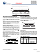

PRELIMINARY
CY14B101Q1
CY14B101Q2
CY14B101Q3
Document #: 001-50091 Rev. *A Page 5 of 22
Note CY14B101Q2/CY14B101Q3 has AutoStore Enabled from
the factory. In CY14B101Q1, V
CAP
pin is not present and
AutoStore option is not available. The Autostore Enable and
Disable instructions to CY14B101Q1 are ignored.
Note If AutoStore is disabled and V
CAP
is not required, leave it
open. V
CAP
pin must never be connected to GND. Power Up
Recall operation cannot be disabled in any case.
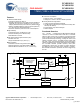
Serial Peripheral Interface
SPI Overview
The SPI is a four-pin interface with Chip Select (CS), Serial Input
(SI), Serial Output (SO) and Serial Clock (SCK) pins.
CY14B101Q1/CY14B101Q2/CY14B101Q3 provides serial
access to nvSRAM through SPI interface. The SPI bus on this
device can run at speeds up to 40 MHz
The SPI is a synchronous serial interface which uses clock and
data pins for memory access and supports multiple devices on
the data bus. A device on SPI bus is activated using a chip select
pin.
The relationship between chip select, clock, and data is dictated
by the SPI mode. This device supports SPI modes 0 and 3. In
both these modes, data is clocked into nvSRAM on rising edge
of SCK starting from the first rising edge after CS
goes active.
The SPI protocol is controlled by opcodes. These opcodes
specify the commands from the bus master to the slave device.
After CS
is activated the first byte transferred from the bus
master is the opcode. Following the opcode, any addresses and
data are then transferred. The CS
must go inactive after an
operation is complete and before a new opcode can be issued.
The commonly used terms used in SPI protocol are given below:
SPI Master
The SPI Master device controls the operations on a SPI bus. An
SPI bus may have only one master with one or more slave
devices. All the slaves share the same SPI bus lines and master
may select any of the slave devices using the Chip Select pin.
All the operations must be initiated by the master activating a
slave device by pulling the CS
pin of the slave LOW. The master
also generates the Serial Clock (SCK) and all the data trans-
mission on SI and SO lines are synchronized with this clock.
SPI Slave
SPI slave device is activated by the master through the Chip
Select line. A slave device gets the Serial Clock (SCK) as an
input from the SPI master and all the communication is synchro-
nized with this clock. SPI slave never initiates a communication
on the SPI bus and acts on the instruction from the master.
CY14B101Q1/CY14B101Q2/CY14B101Q3 operates as a SPI
slave and may share the SPI bus with other SPI slave devices.
Chip Select (CS
)
For selecting any slave device, the master needs to pull down
the corresponding CS
pin. Any instruction can be issued to a
slave device only while the CS
pin is LOW. When the device is
not selected, data through the SI pin is ignored and the serial
output pin (SO) remains in a high impedance state.
Note A new instruction must begin with the falling edge of Chip
Select (CS
). Therefore, only one opcode can be issued for each
active Chip Select cycle.
Serial Clock (SCK)
Serial clock is generated by the SPI master and the communi-
cation is synchronized with this clock after CS
goes LOW.
CY14B101Q1/CY14B101Q2/CY14B101Q3 enables SPI modes
0 and 3 for data communication. In both these modes, the inputs
are latched by the slave device on the rising edge of SCK and
outputs are issued on the falling edge. Therefore, the first rising
edge of SCK signifies the arrival of first bit (MSB) of SPI
instruction on the SI pin. Further, all data inputs and outputs are
synchronized with SCK.
Data Transmission - SI and SO
SPI data bus consists of two lines, SI and SO, for serial data
communication. The SI is also referred to as MOSI (Master Out
Slave In) and SO is referred to as MISO (Master In Slave Out).
The master issues instructions to the slave through the SI pin,
while the slave responds through the SO pin. Multiple slave
devices may share the SI and SO lines as described earlier.
Most Significant Bit (MSB)
The SPI protocol requires that the first bit to be transmitted is the
Most Significant Bit (MSB). This is valid for both address and
data transmission.
The 1 Mbit serial nvSRAM requires a 3-byte address for any read
or write operation. However, since the actual address is only 17
bits, it implies that the first seven bits which are fed in are ignored
by the device. Although these seven bits are ‘don’t care’,
Cypress recommends that these bits are treated as 0s to enable
seamless transition to higher memory densities.
Serial Opcode
After the slave device is selected with CS
going LOW, the first
byte received is treated as the opcode for the intended operation.
CY14B101Q1/CY14B101Q2/CY14B101Q3 uses the standard
opcodes for memory accesses. In addition to the memory
accesses, it provides additional opcodes for the nvSRAM
specific functions: STORE, RECALL, AutoStore Enable, and
AutoStore Disable. Refer to Tabl e 3 on page 7 for details.
Invalid Opcode
If an invalid opcode is received, the opcode is ignored and the
device ignores any additional serial data on the SI pin and no
valid data is sent out on the SO pin. Opcode for a new instruction
is recognized only after the next falling edge of CS
.
Status Register
CY14B101Q1/CY14B101Q2/CY14B101Q3 has an 8-bit status
register. The bits in the status register are used to configure the
SPI bus. These bits are described in Tab l e 5 on page 8.
[+] Feedback