
1 Mbit nvSRAM Specification Sheet

PRELIMINARY
CY14B101Q1
CY14B101Q2
CY14B101Q3
Document #: 001-50091 Rev. *A Page 7 of 22
SPI Operating Features
Power Up
Power up is defined as the condition when the power supply is
turned on and V
CC
crosses Vswitch voltage. During this time, the
Chip Select (CS
) must be allowed to follow the V
CC
voltage.
Therefore, CS
must be connected to V
CC
through a suitable pull
up resistor. As a built-in safety feature, Chip Select (CS
) is both
edge sensitive and level sensitive. After power up, the device is
not selected until a falling edge is detected on Chip Select (CS).
This ensures that Chip Select (CS
) must have been HIGH,
before going Low to start the first operation.
As described earlier, nvSRAM performs a Power Up Recall
operation after power up and therefore, all memory accesses are
disabled for t
RECALL
duration after power up. The HSB pin can
be probed to check the ready or busy status of nvSRAM after
power up.
Power On Reset
A Power On Reset (POR) circuit is included to prevent
inadvertent writes. At power up, the device does not respond to
any instruction until the V
CC
reaches the Power On Reset
threshold voltage (V
SWITCH
). After V
CC
transitions the POR
threshold, the device is internally reset and performs an Power
Up Recall operation. The device is in the following state after
POR:
■ Deselected (after Power up, a falling edge is required on Chip
Select (CS
) before any instructions are started).
■ Standby Power mode
■ Not in the Hold Condition
■ Status register state:
❐ Write Enable (WEN) bit is reset to 0.
❐ WPEN, BP1, BP0 unchanged from previous power down
The WPEN, BP1, and BP0 bits of the Status Register are nonvol-
atile bits and remain unchanged from the previous power down.
Before selecting and issuing instructions to the memory, a valid
and stable V
CC
voltage must be applied. This voltage must
remain valid until the end of the transmission of the instruction.
Power Down
At power down (continuous decay of V
CC
), when V
CC
drops from
the normal operating voltage and below the V
SWITCH
threshold
voltage, the device stops responding to any instruction sent to it.
If a write cycle is in progress during power down, it is allowed
t
DELAY
time to complete after Vcc transitions below V
SWITCH
,
after which all memory accesses are inhibited and a conditional
AutoStore operation is performed (AutoStore is not performed if
no writes have happened since last RECALL cycle). This feature
prevents inadvertent writes to nvSRAM from happening during
power down.
However, to completely avoid the possibility of inadvertent writes
during power down, ensure that the device is deselected and is
in Standby Power Mode, and the Chip Select (CS
) follows the
voltage applied on V
CC
.
Active Power and Standby Power Modes
When Chip Select (CS) is LOW, the device is selected, and is in
the Active Power mode. The device consumes I
CC
current, as
specified in DC Electrical Characteristics on page 13. When Chip
Select (CS
) is HIGH, the device is deselected and the device
goes into the Standby Power mode if a STORE or RECALL cycle
is not in progress. If a STORE or RECALL cycle is in progress,
device goes into the Standby Power Mode after the STORE or
RECALL cycle is completed. In the Standby Power mode, the
current drawn by the device drops to I
SB
.
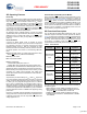
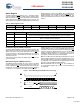
SPI Functional Description
The CY14B101Q1/CY14B101Q2/CY14B101Q3 uses an 8-bit
instruction register. Instructions and their opcodes are listed in
Tab l e 3. All instructions, addresses, and data are transferred with
the MSB first and start with a HIGH to LOW CS
transition. There
are, in all, 12 SPI instructions which provide access to most of
the functions in nvSRAM. Further, the WP
and HOLD pins
provide additional functionality driven through hardware.
The SPI instructions are divided based on their functionality in
the following types:
❐ Status Register Access: WRSR and RDSR instructions
❐ Write Protection Functions: WREN and WRDI instructions
along with WP pin and WEN, BP0, and BP1 bits
❐ SRAM memory Access: READ and WRITE instructions
❐ nvSRAM special instructions: STORE, RECALL, ASENB,
and ASDISB
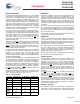
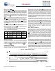
Table 3. Instruction Set
Instruction
Category
Instruction
Name
Opcode Operation
Status Register
Control Instruc-
tions
WREN 0000 0110 Set Write Enable
Latch
WRDI 0000 0100 Reset Write
Enable Latch
RDSR 0000 0101 Read Status
Register
WRSR 0000 0001 Write Status
Register
SRAM
Read/Write
Instructions
READ 0000 0011 Read Data From
Memory Array
WRITE 0000 0010 Write Data To
Memory Array
Special NV
Instructions
STORE 0011 1100 Software STORE
RECALL 0110 0000 Software
RECALL
ASENB 0101 1001 AutoStore Enable
ASDISB 0001 1001 AutoStore Disable
Reserved - Reserved - 0001 1110 Reserved for
Internal use
[+] Feedback