
1 Mbit nvSRAM Specification Sheet

PRELIMINARY
CY14B101Q1
CY14B101Q2
CY14B101Q3
Document #: 001-50091 Rev. *A Page 8 of 22
Status Register
The status register bits are listed in Ta b le 3 . The status register
consists of Ready bit (RDY
) and data protection bits BP1, BP0,
WEN, and WPEN. The RDY
bit can be polled to check the Ready
or Busy status while a nvSRAM STORE cycle is in progress. The
status register can be modified by WRSR instruction and read by
RDSR instruction. However, only WPEN, BP1, and BP0 bits of
the Status Register can be modified by using WRSR instruction.
WRSR instruction has no effect on WEN and RDY
bits. The
default value shipped from the factory for BP1, BP2 and WPEN
bits is ‘0’.
Read Status Register (RDSR) Instruction
The Read Status Register instruction provides access to the
status register. This instruction is used to probe the Write Enable
Status of the device or the Ready status of the device. RDY bit
is set by the device to 1 whenever a STORE cycle is in progress.
The Block Protection and WPEN bits indicate the extent of
protection employed.
This instruction is issued after the falling edge of CS
using the
opcode for RDSR.
Write Status Register (WRSR) Instruction
The WRSR instruction enables the user to write to the Status
register. However, this instruction cannot be used to modify bit 0
and bit 1 (WEN and RDY
). The BP0 and BP1 bits can be used
to select one of four levels of block protection. Further, WPEN bit
can be set to ‘1’ to enable the use of Write Protect (WP) pin.
WRSR instruction is a write instruction and needs writes to be
enabled (WEN bit set to ‘1’) using the WREN instruction before
it is issued. The instruction is issued after the falling edge of CS
using the opcode for WRSR followed by 8 bits of data to be
stored in the Status Register. Since, only bits 2, 3, and 7 can be
modified by WRSR instruction, it is recommended to leave the
other bits as ‘0’ while writing to the Status Register
Note In CY14B101Q1/CY14B101Q2/CY14B101Q3, the values
written to Status Register are saved to nonvolatile memory only
after a STORE operation. If AutoStore is disabled (or while using
CY14B101Q1), any modifications to the Status Register must be
secured by using a Software STORE operation
Note CY14B101Q2 does not have WP
pin. Any modification to
bit 7 of the Status register has no effect on the functionality of
CY14B101Q2.
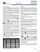
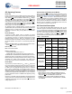
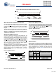
Table 4. Status Register Format
Bit 7 Bit 6 Bit 5 Bit 4 Bit 3 Bit 2 Bit 1 Bit 0
WPEN (0) X X X BP1 (0) BP0 (0) WEN RDY
Table 5. Status Register Bit Definition
Bit Definition Description
Bit 0 (RDY
) Ready Read Only bit indicates the ready status of device to perform a memory access. This bit is
set to “1” by the device while a STORE or Software RECALL cycle is in progress.
Bit 1 (WEN) Write Enable WEN indicates if the device is write-enabled. Setting WEN = '1' enables writes and setting
WEN = '0' disables all write operations
Bit 2 (BP0) Block Protect bit ‘0’ Used for block protection. For details see Tab l e 6 on page 9.
Bit 3 (BP1) Block Protect bit ‘1’ Used for block protection. For details see Tab l e 6 on page 9.
Bit 7 (WPEN) Write Protect Enable bit Used for enabling the function of Write Protect Pin (WP
). For details see Tabl e 7 on page 10.
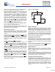
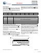
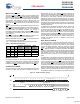
Figure 7. Read Status Register (RDSR) Instruction Timing
CS
SCK
SO
01234567
SI
000001 0
0
1
MSB
LSB
HI-Z
012345 67
Data
LSB
D0D1
D2
D3
D4
D5D6
MSB
D7
[+] Feedback