
1 Mbit nvSRAM Specification Sheet

PRELIMINARY
CY14B101Q1
CY14B101Q2
CY14B101Q3
Document #: 001-50091 Rev. *A Page 9 of 22
Write Protection and Block Protection
CY14B101Q1/CY14B101Q2/CY14B101Q3 provides features
for both software and hardware write protection using WRDI
instruction and WP. Additionally, this device also provides block
protection mechanism through BP0 and BP1 pins of the Status
Register.
The write enable and disable status of the device is indicated by
WEN bit of the status register. The write instructions (WRSR and
WRITE) and nvSRAM special instruction (STORE, RECALL,
ASENB, and ASDISB) need the write to be enabled (WEN bit =
1) before they can be issued.
Write Enable (WREN) Instruction
On power up, the device is always in the write disable state. The
following WRITE, WRSR, or nvSRAM special instruction must
therefore be preceded by a Write Enable instruction. If the device
is not write enabled (WEN = ‘0’), it ignores the write instructions
and returns to the standby state when CS
is brought HIGH. A
new CS
falling edge is required to re-initiate serial communi-
cation. The instruction is issued following the falling edge of CS
.
When this instruction is used, the WEN bit of status register is
set to ‘1’. WEN bit defaults to ‘0’ on power up.
Note After completion of a write instruction (WRSR or WRITE)
or nvSRAM special instruction (STORE, RECALL, ASENB, and
ASDISB) instruction, WEN bit is cleared to ‘0’. This is done to
provide protection from any inadvertent writes. Therefore,
WREN instruction needs to be used before a new write
instruction is issued.
Write Disable (WRDI) Instruction
Write Disable instruction disables the write by clearing the WEN
bit to ‘0’ in order to protect the device against inadvertent writes.
This instruction is issued following falling edge of CS
followed by
opcode for WRDI instruction. The WEN bit is cleared on the
rising edge of CS following a WRDI instruction.
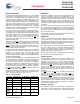
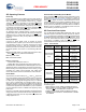
Block Protection
Block protection is provided using the BP0 and BP1 pins of the
Status register. These bits can be set using WRSR instruction
and probed using the RDSR instruction. The nvSRAM is divided
into four array segments. One-quarter, one-half, or all of the
memory segments can be protected. Any data within the
protected segment is read only. Tab le 6 shows the function of
Block Protect bits.
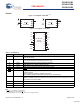
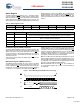
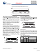
Figure 8. Write Status Register (WRSR) Instruction Timing
CS
SCK
SO
01 23 4567
SI
0000000
1
MSB
LSB
0
0
D2
D3
0
00D7
HI-Z
012345 67
Opcode
Data in
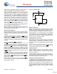
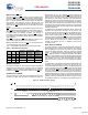
Figure 9. WREN Instruction
0 0 0 0 0 1 1 0
CS
SCK
SI
SO
Hi-Z
0 1 2 3 4 5 6 7
Figure 10. WRDI Instruction
Table 6. Block Write Protect Bits
Level
Status Register
Bits
Array Addresses Protected
BP1 BP0
000 None
1 (1/4) 0 1 0x18000-0x1FFFF
2 (1/2) 1 0 0x10000-0x1FFFF
3 (All) 1 1 0x00000-0x1FFFF
0 00 00 1 00
CS
SCK
SI
SO
Hi-Z
0 1 2 3 4 5 6 7
[+] Feedback