PRELIMINARY CY14B108K, CY14B108M 8 Mbit (1024K x 8/512K x 16) nvSRAM with Real Time Clock Features ■ 20 ns, 25 ns, and 45 ns access times ■ Internally organized as 1024K x 8 (CY14B108K) or 512K x 16 (CY14B108M) ■ Hands off automatic STORE on power down with only a small capacitor ■ STORE to QuantumTrap® nonvolatile elements is initiated by software, device pin, or AutoStore® on power down ■ RECALL to SRAM initiated by software or power up ■ High reliability ■ Infinite Read, Write, and RECALL
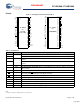
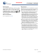
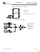
PRELIMINARY CY14B108K, CY14B108M Pinouts Figure 1.
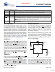
PRELIMINARY CY14B108K, CY14B108M Table 1. Pin Definitions (continued) Pin Name I/O Type INT Output Interrupt Output. Programmable to respond to the clock alarm, the watchdog timer, and the power monitor. Also programmable to either active HIGH (push or pull) or LOW (open drain). Ground Ground for the Device. Must be connected to ground of the system. VSS VCC HSB VCAP Description Power Supply Power Supply Inputs to the Device. 3.0V +20%, –10%. Input/Output Hardware STORE Busy (HSB).
PRELIMINARY power-on-recall, the MPU must be active or the WE held inactive until the MPU comes out of reset. To reduce unnecessary nonvolatile STOREs, AutoStore, and Hardware STORE operations are ignored unless at least one write operation has taken place since the most recent STORE or RECALL cycle. Software initiated STORE cycles are performed regardless of whether a write operation has taken place. The HSB signal is monitored by the system to detect if an AutoStore cycle is in progress.
PRELIMINARY CY14B108K, CY14B108M Table 2.
PRELIMINARY CY14B108K, CY14B108M Data Protection Best Practices The CY14B108K/CY14B108M protects data from corruption during low voltage conditions by inhibiting all externally initiated STORE and write operations. The low voltage condition is detected when VCC is less than VSWITCH. If the CY14B108K/CY14B108M is in a write mode (both CE and WE are LOW) at power up, after a RECALL or STORE, the write is inhibited until the SRAM is enabled after tLZHSB (HSB to output active).
PRELIMINARY Real Time Clock Operation nvTime Operation The CY14B108K/CY14B108M offers internal registers that contain clock, alarm, watchdog, interrupt, and control functions. RTC registers use the last 16 address locations of the SRAM. Internal double buffering of the clock and timer information registers prevents accessing transitional internal clock data during a read or write operation.
PRELIMINARY CY14B108K, CY14B108M calibration registers and the OSCEN bit are not affected by the ‘oscillator failed’ condition. alarm internal flag (AF) is set and an interrupt is generated on INT pin if Alarm Interrupt Enable (AIE) bit is set. The value of OSCF must be reset to ‘0’ when the time registers are written for the first time. This initializes the state of this bit which may have become set when the system was first powered on.
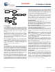
PRELIMINARY Figure 3. Watchdog Timer Block Diagram Clock Divider Oscillator 32,768 KHz 1 Hz 32 Hz Counter Zero Compare WDF Load Register WDS Q D output from the INT pin. In pulse mode, the pulse width is internally fixed at approximately 200 ms. This mode is intended to reset a host microcontroller. In the level mode, the pin goes to its active polarity until the Flags register is read by the user. This mode is used as an interrupt to a host microcontroller.
PRELIMINARY CY14B108K, CY14B108M Figure 4. RTC Recommended Component Configuration Recommended Values Y1 = 32.768 KHz (6 pF) C1 = 21 pF C2 = 21 pF Note: The recommended values for C1 and C2 include board trace capacitance. C1 Y1 C2 Xout Xin Figure 5.
PRELIMINARY CY14B108K, CY14B108M Table 4.
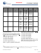
PRELIMINARY CY14B108K, CY14B108M Table 5. Register Map Detail Register CY14B108K CY14B108M 0xFFFFF 0x7FFFF Description Time Keeping - Years D7 D6 D5 D4 D3 D2 10s Years D1 D0 Years Contains the lower two BCD digits of the year. Lower nibble (four bits) contains the value for years; upper nibble (four bits) contains the value for 10s of years. Each nibble operates from 0 to 9. The range for the register is 0–99.
PRELIMINARY CY14B108K, CY14B108M Table 5. Register Map Detail (continued) Register CY14B108K CY14B108M 0xFFFF8 0x7FFF8 OSCEN Description Calibration/Control D7 D6 D5 OSCEN 0 Calibration Sign D4 D3 D2 D1 D0 Calibration Oscillator Enable. When set to 1, the oscillator is stopped. When set to 0, the oscillator runs. Disabling the oscillator saves battery or capacitor power during storage.
PRELIMINARY CY14B108K, CY14B108M Table 5. Register Map Detail (continued) Register CY14B108K CY14B108M 0xFFFF4 0x7FFF4 Description Alarm - Hours D7 D6 M D5 D4 D3 10s Alarm Hours D2 D1 D0 Alarm Hours Contains the alarm value for the hours and the mask bit to select or deselect the hours value. M 0xFFFF3 Match. When this bit is set to 0, the hours value is used in the alarm match. Setting this bit to 1 causes the match circuit to ignore the hours value.
PRELIMINARY CY14B108K, CY14B108M Maximum Ratings Transient Voltage (<20 ns) on Any Pin to Ground Potential .................. –2.0V to VCC + 2.0V Exceeding maximum ratings may impair the useful life of the device. These user guidelines are not tested. Package Power Dissipation Capability (TA = 25°C) ................................................... 1.0W Storage Temperature .................................
PRELIMINARY CY14B108K, CY14B108M Data Retention and Endurance Parameter Description Min Unit DATAR Data Retention 20 Years NVC Nonvolatile STORE Operations 200 K Capacitance In the following table, the capacitance parameters are listed. [13] Parameter Description CIN Input Capacitance COUT Output Capacitance Test Conditions Max Unit 14 pF 14 pF TA = 25°C, f = 1 MHz, VCC = 0 to 3.0V Thermal Resistance In the following table, the thermal resistance parameters are listed.
PRELIMINARY CY14B108K, CY14B108M Table 6. RTC Characteristics Parameters IBAK [14] Description RTC Backup Current Test Conditions Max Units o Min Typ Room Temperature (25 C) 300 nA Hot Temperature (85oC) 450 nA VRTCbat RTC Battery Pin Voltage 1.8 3.0 3.3 V VRTCcap RTC Capacitor Pin Voltage 1.5 3.0 3.6 V tOCS RTC Oscillator Time to Start 1 2 sec Note 14. From either VRTCcap or VRTCbat. Document #: 001-47378 Rev.
PRELIMINARY CY14B108K, CY14B108M AC Switching Characteristics Parameters Cypress Alt Parameters Parameters SRAM Read Cycle tACE tACS [15] tRC tRC tAA tAA [16] tDOE tOE [16] tOH tOHA tLZCE [13, 17] tLZ tHZCE [13, 17] tHZ [13, 17] tLZOE tOLZ tHZOE [13, 17] tOHZ tPU [13] tPA [13] tPD tPS tDBE tLZBE[13] [13] tHZBE SRAM Write Cycle tWC tWC tWP tPWE tSCE tCW tSD tDW tHD tDH tAW tAW tSA tAS tHA tWR [13, 17,18] tHZWE tWZ tLZWE [13, 17] tOW tBW - 20 ns Description Min Chip Enable Access Time Read Cycle Time Add
PRELIMINARY CY14B108K, CY14B108M Switching Waveforms Figure 8. SRAM Read Cycle 2: CE Controlled[3, 15, 19] Address Address Valid tRC tACE CE tHZCE tAA tLZCE tHZOE tDOE OE tHZBE tLZOE tDBE BHE, BLE tLZBE Data Output ICC High Impedance Output Data Valid tPU tPD Active Standby Figure 9.
PRELIMINARY CY14B108K, CY14B108M Switching Waveforms Figure 10. SRAM Write Cycle 2: CE Controlled[3, 18, 19, 20] tWC Address Valid Address tSA tSCE tHA CE tBW BHE, BLE tPWE WE tHD tSD Input Data Valid Data Input High Impedance Data Output Figure 11. SRAM Write Cycle 3: BHE and BLE Controlled[5, 18, 19, 20, 21] (Not applicable for RTC register writes) tWC Address Address Valid tSCE CE tSA tHA tBW BHE, BLE tAW tPWE WE tSD Data Input tHD Input Data Valid High Impedance Data Output Note 21.
PRELIMINARY CY14B108K, CY14B108M AutoStore/Power Up RECALL Parameters 20 ns Description Min 25 ns Max tHRECALL [22] Power Up RECALL Duration tSTORE [23] Min 45 ns Max 20 Min Max 20 Unit 20 ms STORE Cycle Duration 8 8 8 ms tDELAY [24] Time Allowed to Complete SRAM Cycle 20 25 25 ns VSWITCH Low Voltage Trigger Level tVCCRISE VCC Rise Time VHDIS[13] HSB Output Driver Disable Voltage tLZHSB HSB To Output Active Time tHHHD HSB High Active Time 2.65 150 2.65 150 2.
PRELIMINARY CY14B108K, CY14B108M Software Controlled STORE and RECALL Cycle In the following table, the software controlled STORE and RECALL cycle parameters are listed.
PRELIMINARY CY14B108K, CY14B108M Hardware STORE Cycle Parameters 20 ns Description Min tDHSB HSB To Output Active Time when write latch not set tPHSB Hardware STORE Pulse Width 25 ns Max Min 45 ns Max 20 Min 25 15 15 Max 25 15 Unit ns ns Switching Waveforms Figure 15.
PRELIMINARY CY14B108K, CY14B108M Truth Table For SRAM Operations HSB should remain HIGH for SRAM Operations.
PRELIMINARY CY14B108K, CY14B108M Part Numbering Nomenclature CY14 B 108 K ZS P 20 X C T Option: T - Tape & Reel Blank - Std. Pb-Free Temperature: C - Commercial (0 to 70°C) I - Industrial (–40 to 85°C) P - 54 Pin Blank - 44 Pin Speed: 20 - 20 ns 25 - 25 ns 45 - 45 ns Package: ZS - TSOP II Data Bus: K - x8 + RTC M - x16 + RTC Density: 108 - 8 Mb Voltage: B - 3.0V NVSRAM 14 - AutoStore + Software STORE + Hardware STORE Cypress Document #: 001-47378 Rev.
PRELIMINARY CY14B108K, CY14B108M Ordering Information Speed (ns) 20 25 45 Ordering Code Package Diagram Package Type CY14B108K-ZS20XCT 51-85087 44-pin TSOPII CY14B108K-ZS20XC 51-85087 44-pin TSOPII CY14B108K-ZS20XIT 51-85087 44-pin TSOPII CY14B108K-ZS20XI 51-85087 44-pin TSOPII CY14B108M-ZSP20XCT 51-85160 54-pin TSOPII CY14B108M-ZSP20XC 51-85160 54-pin TSOPII CY14B108M-ZSP20XIT 51-85160 54-pin TSOPII CY14B108M-ZSP20XI 51-85160 54-pin TSOPII CY14B108K-ZS25XCT 51-85087 44-pin
PRELIMINARY CY14B108K, CY14B108M Package Diagrams Figure 17. 44-Pin TSOP II (51-85087) DIMENSION IN MM (INCH) MAX MIN. PIN 1 I.D. 1 23 10.262 (0.404) 10.058 (0.396) 11.938 (0.470) 11.735 (0.462) 22 EJECTOR PIN 44 TOP VIEW 0.800 BSC (0.0315) OR E K X A SG BOTTOM VIEW 0.400(0.016) 0.300 (0.012) 10.262 (0.404) 10.058 (0.396) BASE PLANE 0.210 (0.0083) 0.120 (0.0047) 0°-5° 0.10 (.004) 0.150 (0.0059) 0.050 (0.0020) 1.194 (0.047) 0.991 (0.039) 18.517 (0.729) 18.313 (0.721) SEATING PLANE 0.
PRELIMINARY Package Diagrams CY14B108K, CY14B108M (continued) Figure 18. 54-Pin TSOP II (51-85160) 51-85160 ** Document #: 001-47378 Rev.
PRELIMINARY CY14B108K, CY14B108M Document History Page Document Title: CY14B108K/CY14B108M 8 Mbit (1024K x 8/512K x 16) nvSRAM with Real Time Clock Document Number: 001-47378 Rev. ECN No. Orig. of Change Submission Date ** 2681767 GVCH/PYRS 04/01/09 Description of Change New Data Sheet Sales, Solutions, and Legal Information Worldwide Sales and Design Support Cypress maintains a worldwide network of offices, solution centers, manufacturer’s representatives, and distributors.