
nvSRAM Specification Sheet
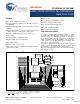

PRELIMINARY
CY14B108K, CY14B108M
Document #: 001-47378 Rev. ** Page 4 of 29
power-on-recall, the MPU must be active or the WE
held inactive
until the MPU comes out of reset.
To reduce unnecessary nonvolatile STOREs, AutoStore, and
Hardware STORE operations are ignored unless at least one
write operation has taken place since the most recent STORE or
RECALL cycle. Software initiated STORE cycles are performed
regardless of whether a write operation has taken place. The
HSB signal is monitored by the system to detect if an AutoStore
cycle is in progress.
Hardware STORE (HSB) Operation
The CY14B108K/CY14B108M provides the HSB pin to control
and acknowledge the STORE operations. The HSB
pin is used
to request a Hardware STORE cycle. When the HSB
pin is driven
LOW, the CY14B108K/CY14B108M conditionally initiates a
STORE operation after t
DELAY
. An actual STORE cycle begins
only if a write to the SRAM has taken place since the last STORE
or RECALL cycle. The HSB pin also acts as an open drain driver
that is internally driven LOW to indicate a busy condition when
the STORE (initiated by any means) is in progress.
SRAM read and write operations, that are in progress when HSB
is driven LOW by any means, are given time t
DELAY
to complete
before the STORE operation is initiated. However, any SRAM
write cycles requested after HSB
goes LOW are inhibited until
HSB
returns HIGH. In case the write latch is not set, HSB is not
driven LOW by the CY14B108K/CY14B108M but any SRAM
read and write cycles are inhibited until HSB
is returned HIGH by
MPU or external source.
During any STORE operation, regardless of how it is initiated,
the CY14B108K/CY14B108M continues to drive the HSB
pin
LOW, releasing it only when the STORE is complete. Upon
completion of the STORE operation, the
CY14B108K/CY14B108M remains disabled until the HSB
pin
returns HIGH. Leave the HSB
unconnected if it is not used.
Hardware RECALL (Power Up)
During power up or after any low power condition
(V
CC
<V
SWITCH
), an internal RECALL request is latched. When
V
CC
again exceeds the V
SWITCH
on powerup, a RECALL cycle
is automatically initiated and takes t
HRECALL
to complete. During
this time, the HSB
pin is driven LOW by the HSB driver and all
reads and writes to nvSRAM are inhibited.
Software STORE
Data is transferred from the SRAM to the nonvolatile memory by
a software address sequence. The CY14B108K/CY14B108M
Software STORE cycle is initiated by executing sequential CE
or
OE
controlled read cycles from six specific address locations in
exact order. During the STORE cycle, an erase of the previous
nonvolatile data is first performed, followed by a program of the
nonvolatile elements. After a STORE cycle is initiated, further
input and output are disabled until the cycle is completed.
Because a sequence of reads from specific addresses is used
for STORE initiation, it is important that no other read or write
accesses intervene in the sequence, or the sequence is aborted
and no STORE or RECALL takes place.
To initiate the Software STORE cycle, the following read
sequence must be performed:
1. Read address 0x4E38 Valid READ
2. Read address 0xB1C7 Valid READ
3. Read address 0x83E0 Valid READ
4. Read address 0x7C1F Valid READ
5. Read address 0x703F Valid READ
6. Read address 0x8FC0 Initiate STORE cycle
The software sequence may be clocked with CE
or OE controlled
reads. Both CE
and OE must be toggled for the sequence to be
executed. After the sixth address in the sequence is entered, the
STORE cycle starts and the chip is disabled. It is important to use
read cycles and not write cycles in the sequence. The SRAM is
activated again for read and write operations after the t
STORE
cycle time.
Software RECALL
Data is transferred from the nonvolatile memory to the SRAM by
a software address sequence. A software RECALL cycle is
initiated with a sequence of read operations in a manner similar
to the Software STORE initiation. To initiate the RECALL cycle,
perform the following sequence of CE
or OE controlled read
operations:
1. Read address 0x4E38 Valid READ
2. Read address 0xB1C7 Valid READ
3. Read address 0x83E0 Valid READ
4. Read address 0x7C1F Valid READ
5. Read address 0x703F Valid READ
6. Read address 0x4C63 Initiate RECALL cycle
Internally, RECALL is a two step procedure. First, the SRAM data
is cleared; then, the nonvolatile information is transferred into the
SRAM cells. After the t
RECALL
cycle time, the SRAM is again
ready for read and write operations. The RECALL operation
does not alter the data in the nonvolatile elements.
[+] Feedback