
Specifications


CY14B108K, CY14B108M
Document #: 001-47378 Rev. *D Page 22 of 31
AutoStore/Power Up RECALL
Parameters Description
CY14B108K/CY14B108M
Unit
Min Max
t
HRECALL
[22]
Power Up RECALL Duration 20 ms
t
STORE
[23]
STORE Cycle Duration 8 ms
t
DELAY
[24]
Time Allowed to Complete SRAM Write Cycle 25 ns
V
SWITCH
Low Voltage Trigger Level 2.65 V
t
VCCRISE
[12]
V
CC
Rise Time 150 μs
V
HDIS
[12]
HSB Output Disable Voltage 1.9 V
t
LZHSB
[12]
HSB To Output Active Time 5 μs
t
HHHD
[12]
HSB High Active Time 500 ns
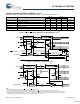
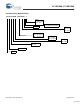
Switching Waveforms
Figure 12. AutoStore or Power Up RECALL
[25]
V
SWITCH
V
HDIS
V
VCCRISE
t
STORE
t
STORE
t
HHHD
t
HHHD
t
DELAY
t
DELAY
t
LZHSB
t
LZHSB
t
HRECALL
t
HRECALL
HSB OUT
AutoStore
POWER-
UP
RECALL
Read & Write
Inhibited
(
RWI)
POWER-UP
RECALL
Read & Write
BROWN
OUT
AutoStore
POWER-UP
RECALL
Read & Write
POWER
DOWN
AutoStore
Note
Note
Note
V
CC
23
23
26
Notes
22. t
HRECALL
starts from the time V
CC
rises above V
SWITCH.
23. If an SRAM write has not taken place since the last nonvolatile cycle, no AutoStore or Hardware STORE takes place.
24. On a Hardware Store and AutoStore initiation, SRAM write operation continues to be enabled for time t
DELAY
.
25. Read and Write cycles are ignored during STORE, RECALL, and while V
CC
is below V
SWITCH.
26. HSB pin is driven HIGH to V
CC
only by internal 100 kΩ resistor, HSB driver is disabled.
[+] Feedback