
Static RAM Specification Sheet
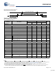
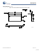

CY62128EV30
MoBL® 1 Mbit (128K x 8) Static RAM
Cypress Semiconductor Corporation • 198 Champion Court • San Jose, CA 95134-1709 • 408-943-2600
Document #: 38-05579 Rev. *D Revised March 28, 2008
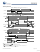
Features
■ Very high speed: 45 ns
❐ Temperature ranges:
• Industrial: –40°C to +85°C
• Automotive-A: –40°C to +85°C
• Automotive-E: –40°C to +125°C
■ Wide voltage range: 2.20V – 3.60V
■ Pin compatible with CY62128DV30
■ Ultra low standby power
❐ Typical standby current: 1 μA
❐ Maximum standby current: 4 μA
■ Ultra low active power
❐ Typical active current: 1.3 mA @ f = 1 MHz
■ Easy memory expansion with CE
1
, CE
2
and OE features
■ Automatic power down when deselected
■ CMOS for optimum speed and power
■ Offered in Pb-free 32-pin SOIC, 32-pin TSOP I, and 32-pin
STSOP packages
Functional Description
The CY62128EV30
[1]
is a high performance CMOS static RAM
module organized as 128K words by 8 bits. This device features
advanced circuit design to provide ultra low active current. This
is ideal for providing More Battery Life™ (MoBL
®
) in portable
applications such as cellular telephones. The device also has an
automatic power down feature that significantly reduces power
consumption when addresses are not toggling. Placing the
device into standby mode reduces power consumption by more
than 99% when deselected (CE
1
HIGH or CE
2
LOW). The eight
input and output pins (IO
0
through IO
7
) are placed in a high
impedance state when the device is deselected (CE
1
HIGH or
CE
2
LOW), the outputs are disabled (OE HIGH), or a write
operation is in progress (CE
1
LOW and CE
2
HIGH and WE
LOW).
To write to the device, take Chip Enable (CE
1
LOW and CE
2
HIGH) and Write Enable (WE) inputs LOW. Data on the eight IO
pins is then written into the location specified on the Address pin
(A
0
through A
16
).
To read from the device, take Chip Enable (CE
1
LOW and CE
2
HIGH) and Output Enable (OE) LOW while forcing Write Enable
(WE
) HIGH. Under these conditions, the contents of the memory
location specified by the address pins appear on the IO pins.
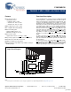
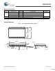
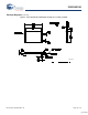
A
0
IO
0
IO
7
IO
1
IO
2
IO
3
IO
4
IO
5
IO
6
A
1
A
2
A
3
A
4
A
5
A
6
A
7
A
8
A
9
A
12
SENSE AMPS
POWER
DOWN
WE
OE
A
13
A
14
A
15
A
16
ROW DECODER
COLUMN DECODER
128K x 8
ARRAY
INPUT BUFFER
A
10
A
11
CE
1
CE
2
Logic Block Diagram
Note
1. For best practice recommendations, refer to the Cypress application note “System Design Guidelines” at http://www.cypress.com.
[+] Feedback