
4-Mbit Static RAM Specification Sheet
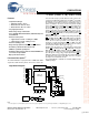

CY62147DV30
Document #: 38-05340 Rev. *F Page 3 of 12
Maximum Ratings
(Above which the useful life may be impaired. For user guide-
lines, not tested.)
Storage Temperature .................................–65°C to +150°C
Ambient Temperature with
Power Applied.............................................–55°C to +125°C
Supply Voltage to Ground
Potential......................................–0.3V to + V
CC(MAX)
+ 0.3V
DC Voltage Applied to Outputs
in High-Z State
[6,7]
..........................–0.3V to V
CC(MAX)
+ 0.3V
DC Input Voltage
[6,7]
..................... –0.3V to V
CC(MAX)
+ 0.3V
Output Current into Outputs (LOW)............................. 20 mA
Static Discharge Voltage........................................... >2001V
(per MIL-STD-883, Method 3015)
Latch-up Current......................................................>200 mA
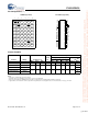
Operating Range
Device Range
Ambient
Temperature
[T
A
]
[9]
V
CC
CY62147DV30L Automotive-E –40°C to +125°C 2.20V
to
3.60V
CY62147DV30LL Industrial –40°C to +85°C
Automotive-A –40°C to +85°C
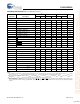
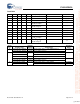
Electrical Characteristics (Over the Operating Range)
Parameter Description Test Conditions
–45 –55/–70
UnitMin. Typ.
[5]
Max. Min. Typ.
[5]
Max.
V
OH
Output HIGH
Voltage
I
OH
= –0.1 mA V
CC
= 2.20V 2.0 2.0 V
I
OH
= –1.0 mA V
CC
= 2.70V 2.4 2.4 V
V
OL
Output LOW
Voltage
I
OL
= 0.1 mA V
CC
= 2.20V 0.4 0.4 V
I
OL
= 2.1 mA V
CC
= 2.70V 0.4 0.4 V
V
IH
Input HIGH
Voltage
V
CC
= 2.2V to 2.7V 1.8 V
CC
+ 0.3V 1.8 V
CC
+ 0.3V V
V
CC
= 2.7V to 3.6V 2.2 V
CC
+ 0.3V 2.2 V
CC
+ 0.3V V
V
IL
Input LOW
Voltage
V
CC
= 2.2V to 2.7V –0.3 0.6 –0.3 0.6 V
V
CC
= 2.7V to 3.6V –0.3 0.8 –0.3 0.8 V
I
IX
Input Leakage
Current
GND < V
I
< V
CC
Ind’l
–1 +1 –1 +1 µA
Auto-A
[9]
–1 +1 µA
Auto-E
[9]
–4 +4 µA
I
OZ
Output
Leakage
Current
GND <
V
O
< V
CC
,
Output Disabled
Ind’l
–1 +1 –1 +1 µA
Auto-A
[9]
–1 +1 µA
Auto-E
[9]
–4 +4 µA
I
CC
V
CC
Operating
Supply
Current
f = f
MAX
= 1/t
RC
V
CC
= V
CCmax
I
OUT
= 0 mA
CMOS levels
10 20 8 15 mA
f = 1 MHz 1.5 3 1.5 3 mA
I
SB1
Automatic CE
Power-Down
Current —
CMOS Inputs
CE
> V
CC
−0.2V,
V
IN
>V
CC
–0.2V, V
IN
<0.2V)
f = f
MAX
(Address and
Data Only),
f = 0 (OE
, WE, BHE and
BLE
), V
CC
= 3.60V
Ind’l LL 8 8 µA
Auto-A
[9]
LL 8
Auto-E
[9]
L25
I
SB2
Automatic CE
Power-Down
Current —
CMOS Inputs
CE > V
CC
– 0.2V,
V
IN
> V
CC
– 0.2V or
V
IN
< 0.2V,
f = 0, V
CC
= 3.60V
Ind’l LL 8 8 µA
Auto-A
[9]
LL 8
Auto-E
[9]
L25
Notes:
6. V
IL(min.)
= –2.0V for pulse durations less than 20 ns.
7. V
IH(max.)
= V
CC
+ 0.75V for pulse durations less than 20 ns.
8. Full device AC operation assumes a 100-µs ramp time from 0 to V
CC
(min) and 200-µs wait time after V
CC
stabilization.
9. Auto-A is available in –70 and Auto-E is available in –55.
[+] Feedback