
Low Skew Clock Buffer Specification Sheet


CY7B9910
CY7B9920
Document Number: 38-07135 Rev. *B Page 2 of 11
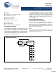
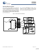
Pin Configuration
Test Mode
The TEST input is a three level input. In normal system operation, this pin is connected to ground, allowing the CY7B9910 and
CY7B9920 to operate as described in Block Diagram Description. For testing purposes, any of the three level inputs can have a
removable jumper to ground or be tied LOW through a 100W resistor. This enables an external tester to change the state of these pins.
If the TEST input is forced to its MID or HIGH state, the device operates with its internal phase locked loop disconnected and input
levels supplied to REF directly control all outputs. Relative output-to-output functions are the same as in normal mode.
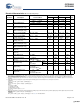
Pin Definitions
Signal Name IO Description
REF I Reference frequency input.This input supplies the frequency and timing against which all functional
variations are measured.
FB I PLL feedback input (typically connected to one of the eight outputs).
FS
[1,2,3]
I Three level frequency range select.
TEST I Three level select. See TEST MODE.
Q[0..7] O Clock outputs.
V
CCN
PWR Power supply for output drivers.
V
CCQ
PWR Power supply for internal circuitry.
GND PWR Ground.
Q4
Q2
REF
V
CCQ
FS
NC
V
CCQ
V
CCN
Q0
Q1
GND
Q3
V
CCN
GND
TEST
NC
GND
V
CCN
Q7
Q6
GND
Q5
V
CCN
FB
SOIC
Top View
1
2
3
4
5
6
7
8
9
10
11
12
15
16
17
18
19
20
24
23
22
21
13
14
7B9910
7B9920
Notes
1. For all three state inputs, HIGH indicates a connection to VCC, LOW indicates a connection to GND, and MID indicates an open connection. Internal termination
circuitry holds an unconnected input to VCC/2.
2. The level to be set on FS is determined by the “normal” operating frequency (fNOM) of the VCO (see Logic Block Diagram). The frequency appearing at the REF
and FB inputs are fNOM when the output connected to FB is undivided. The frequency of the REF and FB inputs are fNOM/X when the device is configured for a
frequency multiplication by using external division in the feedback path of value X.
3. When the FS pin is selected HIGH, the REF input must not transition upon power up until VCC reached 4.3V.
[+] Feedback [+] Feedback