
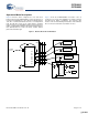
Low Skew Clock Buffer Specification Sheet
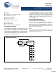


CY7B9910
CY7B9920
Document Number: 38-07135 Rev. *B Page 4 of 11
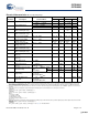
Electrical Characteristics Over the Operating Range
CY7B9910 CY7B9920
Parameter Description Test Conditions Min Max Min Max Unit
V
OH
Output HIGH Voltage V
CC
= Min, I
OH
= –16 mA 2.4 V
V
CC
= Min, I
OH
=–40 mA V
CC
–0.75
V
OL
Output LOW Voltage V
CC
= Min, I
OL
= 46 mA 0.45 V
V
CC
= Min, I
OL
= 46 mA 0.45
V
IH
Input HIGH Voltage
(REF and FB inputs only)
2.0 V
CC
V
CC
–
1.35
V
CC
V
V
IL
Input LOW Voltage
(REF and FB inputs only)
–0.5 0.8 –0.5 1.35 V
V
IHH
Three Level Input HIGH
Voltage (Test, FS)
[4]
Min ≤ V
CC
≤ Max V
CC
– 1V V
CC
V
CC
– 1V V
CC
V
V
IMM
Three Level Input MID
Voltage (Test, FS)
[4]
Min ≤ V
CC
≤ Max V
CC
/2 –
500 mV
V
CC
/2 +
500 mV
V
CC
/2 –
500 mV
V
CC
/2 +
500 mV
V
V
ILL
Three Level Input LOW
Voltage (Test, FS)
[4]
Min ≤ V
CC
≤ Max 0.0 1.0 0.0 1.0 V
I
IH
Input HIGH Leakage Current
(REF and FB inputs only)
V
CC
= Max, V
IN
= Max 10 10 μA
I
IL
Input LOW Leakage Current
(REF and FB inputs only)
V
CC
= Max, V
IN
= 0.4V –500 –500 μA
I
IHH
Input HIGH Current
(Test, FS)
V
IN
= V
CC
200 200 μA
I
IMM
Input MID Current
(Test, FS)
V
IN
= V
CC
/2 –50 50 –50 50 μA
I
ILL
Input LOW Current
(Test, FS)
V
IN
= GND –200 –200 μA
I
OS
Output Short Circuit
Current
[5]
V
CC
= Max, V
OUT
= GND (25
°C only)
–250 N/A mA
I
CCQ
Operating Current Used by
Internal Circuitry
V
CCN
= V
CCQ
= Max All
Input
Selects Open
Com’l 85 85 mA
Mil/Ind 90 90
I
CCN
Output Buffer Current per
Output Pair
[6]
V
CCN
= V
CCQ
= Max
I
OUT
= 0 mA
Input Selects Open, f
MAX
14 19 mA
PD Power Dissipation per
Output Pair
[7]
V
CCN
= V
CCQ
= Max
I
OUT
= 0 mA
Input Selects Open, f
MAX
78 104
[5]
mW
Notes
4. These inputs are normally wired to VCC, GND, or left unconnected (actual threshold voltages vary as a percentage of VCC). Internal termination resistors hold
unconnected inputs at VCC/2. If these inputs are switched, the function and timing of the outputs may glitch and the PLL may require an additional tLOCK time
before all data sheet limits are achieved.
5. Tested one output at a time, output shorted for less than one second, less than 10% duty cycle. Room temperature only. CY7B9920 outputs are not short circuit
protected.
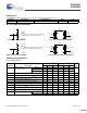
6. Total output current per output pair is approximated by the following expression that includes device current plus load current:
CY7B9910:
ICCN = [(4 + 0.11F) + [((835 – 3F)/Z) + (.0022FC)]N] x 1.1
CY7B9920:
ICCN = [(3.5+.17F) + [((1160 – 2.8F)/Z) + (.0025FC)]N] x 1.1
Where
F = frequency in MHz
C = capacitive load in pF
Z = line impedance in ohms
N = number of loaded outputs; 0, 1, or 2
FC = F < C.
7. Total power dissipation per output pair is approximated by the following expression that includes device power dissipation plus power dissipation due to the load circuit:
CY7B9910:
PD = [(22 + 0.61F) + [((1550 – 2.7F)/Z) + (.0125FC)]N] x 1.1
CY7B9920:
PD = [(19.25+ 0.94F) + [((700 + 6F)/Z) + (.017FC)]N] x 1.1.See note 3 for variable definition.
[+] Feedback [+] Feedback