
Low Skew Clock Buffer Specification Sheet
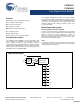


CY7B9910
CY7B9920
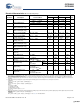
Document Number: 38-07135 Rev. *B Page 6 of 11
CY7B9910–5 CY7B9920–5
Parameter Description Min Typ Max Min Typ Max Unit
f
NOM
Operating Clock
Frequency in MHz
FS = LOW
[1, 2]
15 30 15 30 MHz
FS = MID
[1, 2]
25 50 25 50
FS = HIGH
[1, 2, 3]
40 80 40 80
[12]
t
RPWH
REF Pulse Width HIGH 5.0 5.0 ns
t
RPWL
REF Pulse Width LOW 5.0 5.0 ns
t
SKEW
Zero Output Skew (All Outputs)
[13, 14]
0.25 0.5 0.25 0.5 ns
t
DEV
Device-to-Device Skew
[8, 15]
1.0 1.0 ns
t
PD
Propagation Delay, REF Rise to FB Rise –0.5 0.0 +0.5 –0.5 0.0 +0.5 ns
t
ODCV
Output Duty Cycle Variation
[16]
–1.0 0.0 +1.0 –1.0 0.0 +1.0 ns
t
ORISE
Output Rise Time
[17, 18
0.15 1.0 1.5 0.5 2.0 3.0 ns
t
OFALL
Output Fall Time
[17, 18]
0.15 1.0 1.5 0.5 2.0 3.0 ns
t
LOCK
PLL Lock Time
[19]
0.5 0.5 ms
t
JR
Cycle-to-Cycle Output Jitter Peak to Peak
[8]
200 200 ps
RMS
[8]
25 25 ps
Notes
8. Guaranteed by statistical correlation. Tested initially and after any design or process changes that may affect these parameters.
9. CMOS output buffer current and power dissipation specified at 50 MHz reference frequency.
10. Applies to REF and FB inputs only.
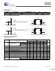
11. Test measurement levels for the CY7B9910 are TTL levels (1.5V to 1.5V). Test measurement levels for the CY7B9920 are CMOS levels (VCC/2 to VCC/2). Test
conditions assume signal transition times of 2ns or less and output loading as shown in the AC Test Loads and Waveforms unless otherwise specified.
12. Except as noted, all CY7B9920–2 and –5 timing parameters are specified to 80 MHz with a 30 pF load.
13. tSKEW is defined as the time between the earliest and the latest output transition among all outputs when all are loaded with 50 pF and terminated with 50Ω to
2.06V (CY7B9910) or VCC/2 (CY7B9920).
14. tSKEW is defined as the skew between outputs.
15. tDEV is the output-to-output skew between any two outputs on separate devices operating under the same conditions (VCC, ambient temperature, air flow, and
so on).
16. tODCV is the deviation of the output from a 50% duty cycle.
17. Specified with outputs loaded with 30 pF for the CY7B99X0–2 and –5 devices and 50 pF for the CY7B99X0–7 devices. Devices are terminated through 50Ω to
2.06V (CY7B9910) or VCC/2 (CY7B9920).
18. tORISE and tOFALL measured between 0.8V and 2.0V for the CY7B9910 or 0.8VCC and 0.2VCC for the CY7B9920.
19. tLOCK is the time that is required before synchronization is achieved. This specification is valid only after VCC is stable and within normal operating limits. This
parameter is measured from the application of a new signal or frequency at REF or FB until tPD is within specified limits.
[+] Feedback [+] Feedback