
Low Skew Clock Buffer Specification Sheet


CY7B9910
CY7B9920
Document Number: 38-07135 Rev. *B Page 9 of 11
Operational Mode Descriptions
Figure 2 shows the device configured as a zero skew clock
buffer. In this mode the 7B9910/9920 is used as the basis for a
low skew clock distribution tree. The outputs are aligned and may
each drive a terminated transmission line to an independent
load. The FB input is tied to any output and the operating
frequency range is selected with the FS pin. The low skew speci-
fication, coupled with the ability to drive terminated transmission
lines (with impedances as low as 50 ohms), enables efficient
printed circuit board design.
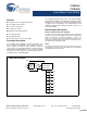
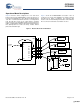
Figure 1 shows the CY7B9910/9920 connected in series to
construct a zero skew clock distribution tree between boards.
Cascaded clock buffers accumulates low frequency jitter
because of the non-ideal filtering characteristics of the PLL filter.
Do not connect more than two clock buffers in series.
Figure 3. Board-to-Board Clock Distribution
SYSTEM
CLOCK
Z
0
FB
REF
FS
TEST
REF
REF
FS
FB
LOAD
LOAD
LOAD
LOAD
LOAD
TEST
Z
0
Z
0
Z
0
Q0
Q1
Q2
Q3
Q4
Q5
Q6
Q7
Q0
Q1
Q2
Q3
Q4
Q5
Q6
Q7
[+] Feedback [+] Feedback