
Low Skew Clock Buffer Specification Sheet

CY7B9910
CY7B9920
Low Skew Clock Buffer
Cypress Semiconductor Corporation • 198 Champion Court • San Jose, CA 95134-1709 • 408-943-2600
Document Number: 38-07135 Rev. *B Revised August 07, 2007
Features
■ All outputs skew <100 ps typical (250 max.)
■ 15 to 80 MHz output operation
■ Zero input to output delay
■ 50% duty cycle outputs
■ Outputs drive 50Ω terminated lines
■ Low operating current
■ 24-pin SOIC package
■ Jitter:<200 ps peak to peak, <25 ps RMS
Functional Description
The CY7B9910 and CY7B9920 Low Skew Clock Buffers offer
low skew system clock distribution. These multiple output clock
drivers optimize the timing of high performance computer
systems. Each of the eight individual drivers can drive terminated
transmission lines with impedances as low as 50Ω. They deliver
minimal and specified output skews and full swing logic levels
(CY7B9910 TTL or CY7B9920 CMOS).
The completely integrated PLL enables “zero delay” capability.
External divide capability, combined with the internal PLL, allows
distribution of a low frequency clock that is multiplied by virtually
any factor at the clock destination. This facility minimizes clock
distribution difficulty while allowing maximum system clock
speed and flexibility.
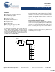
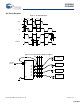
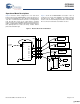
Block Diagram Description
Phase Frequency Detector and Filter
The Phase Frequency Detector and Filter blocks accept inputs
from the reference frequency (REF) input and the feedback (FB)
input and generate correction information to control the
frequency of the Voltage Controlled Oscillator (VCO). These
blocks, along with the VCO, form a Phase Locked Loop (PLL)
that tracks the incoming REF signal.
VCO
The VCO accepts analog control inputs from the PLL filter block
and generates a frequency. The operational range of the VCO is
determined by the FS control pin.
TEST
FB
REF
VOLTAGE
CONTROLLED
OSCILLATOR
FS
Q0
FILTER
PHASE
FREQ
DET
Q1
Q2
Q3
Q4
Q5
Q6
Q7
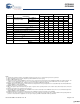
Logic Block Diagram
[+] Feedback [+] Feedback