
Dual-Port Static RAM Specification Sheet

CY7C027V/027VN/027AV/028V
CY7C037V/037AV/038V
Document #: 38-06078 Rev. *B Page 7 of 18
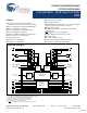
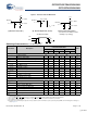
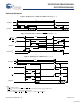
Figure 3. AC Test Loads and Waveforms
3.0V
GND
90%
90%
10%
3ns
3
ns
10%
ALL INPUTPULSES
(a) Normal Load (Load
1)
R1 = 590Ω
3.3V
OUTPUT
R2 = 435Ω
C= 30
pF
V
TH
=1.4V
OUTPUT
C= 30 pF
(b) Thévenin Equivalent (Load 1)
(c) Three-State Delay(Load 2)
R1 = 590Ω
R2 = 435Ω
3.3V
OUTPUT
C= 5pF
R
TH
= 250Ω
≤
≤
including scope and jig)
(Used for t
LZ
, t
HZ
, t
HZWE
, & t
LZWE
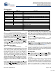
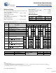
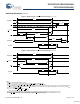
Switching Characteristics
Over the Operating Range
[6]
Parameter Description
CY7C027V/027VN/027AV/028V/
CY7C037V/037AV/038V
Unit
-15 -20 -25
Min Max Min Max Min Max
Read Cycle
t
RC
Read Cycle Time 15 20 25 ns
t
AA
Address to Data Valid 15 20 25 ns
t
OHA
Output Hold From Address Change 3 3 3 ns
t
ACE
[7]
CE LOW to Data Valid 15 20 25 ns
t
DOE
OE LOW to Data Valid 10 12 13 ns
t
LZOE
[8, 9, 10]
OE LOW to Low Z 3 3 3 ns
t
HZOE
[8, 9, 10]
OE HIGH to High Z 10 12 15 ns
t
LZCE
[8, 9, 10]
CE LOW to Low Z 3 3 3 ns
t
HZCE
[8, 9, 10]
CE HIGH to High Z 10 12 15 ns
t
PU
[10]
CE LOW to Power Up 0 0 0 ns
t
PD
[10]
CE HIGH to Power Down 15 20 25 ns
t
ABE
[7]
Byte Enable Access Time 15 20 25 ns
Write Cycle
t
WC
Write Cycle Time 15 20 25 ns
t
SCE
[7]
CE LOW to Write End 12 16 20 ns
t
AW
Address Valid to Write End 12 16 20 ns
t
HA
Address Hold From Write End 0 0 0 ns
t
SA
[7]
Address Setup to Write Start 0 0 0 ns
t
PWE
Write Pulse Width 12 17 22 ns
t
SD
Data Setup to Write End 10 12 15 ns
Notes
6. Test conditions assume signal transition time of 3 ns or less, timing reference levels of 1.5V, input pulse levels of 0 to 3.0V, and output loading of the specified I
OI
/I
OH
and 30 pF load capacitance.
7. To access RAM, CE
=L, UB=L, SEM=H. To access semaphore, CE=H and SEM=L. Either condition must be valid for the entire t
SCE
time.
8. At any given temperature and voltage condition for any given device, t
HZCE
is less than t
LZCE
and t
HZOE
is less than t
LZOE
.
9. Test conditions used are Load 2.
10. This parameter is guaranteed by design, but it is not production tested. For information on port-to-port delay through RAM cells from writing port to reading port,
refer to Figure 11.
[+] Feedback