
Dual-Port Static RAM Specification Sheet

CY7C027V/027VN/027AV/028V
CY7C037V/037AV/038V
Document #: 38-06078 Rev. *B Page 8 of 18
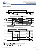
Data Retention Mode
The CY7C027V/027VN/027AV/028V and
CY7037V/037AV/038V are designed with battery backup in
mind. Data retention voltage and supply current are guaranteed
over temperature. The following rules ensure data retention:
1. Chip enable (CE) must be held HIGH during data retention, within
V
CC
to V
CC
– 0.2V.
2. CE
must be kept between V
CC
– 0.2V and 70% of V
CC
during
the power up and power down transitions.
3. The RAM can begin operation >t
RC
after V
CC
reaches the mini-
mum operating voltage (3.0 volts).
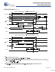
t
HD
Data Hold From Write End 0 0 0 ns
t
HZWE
[9, 10]
R/W LOW to High Z 10 12 15 ns
t
LZWE
[9 ,10]
R/W HIGH to Low Z 3 3 3 ns
t
WDD
[36]
Write Pulse to Data Delay 30 40 50 ns
t
DDD
[36]
Write Data Valid to Read Data Valid 25 30 35 ns
Busy Timing
[11]
t
BLA
BUSY LOW from Address Match 15 20 20 ns
t
BHA
BUSY HIGH from Address Mismatch 15 20 20 ns
t
BLC
BUSY LOW from CE LOW 15 20 20 ns
t
BHC
BUSY HIGH from CE HIGH 15 16 17 ns
t
PS
Port Setup for Priority 5 5 5 ns
t
WB
R/W HIGH after BUSY (Slave) 0 0 0 ns
t
WH
R/W HIGH after BUSY HIGH (Slave) 13 15 17 ns
t
BDD
[13]
BUSY HIGH to Data Valid 15 20 25 ns
Interrupt Timing
[11]
t
INS
INT Set Time 15 20 20 ns
t
INR
INT Reset Time 15 20 20 ns
Semaphore Timing
t
SOP
SEM Flag Update Pulse (OE or SEM)101012ns
t
SWRD
SEM Flag Write to Read Time 5 5 5 ns
t
SPS
SEM Flag Contention Window 5 5 5 ns
t
SAA
SEM Address Access Time 15 20 25 ns
Switching Characteristics
Over the Operating Range
[6]
(continued)
Parameter Description
CY7C027V/027VN/027AV/028V/
CY7C037V/037AV/038V
Unit
-15 -20 -25
Min Max Min Max Min Max
Timing
Parameter Test Conditions
[14]
Max Unit
ICC
DR1
At VCC
DR
= 2V 50 μA
Data Retention Mode
3.0V
3.0V
V
CC
> 2.0V
V
CC
to V
CC
– 0.2V
V
CC
CE
t
RC
V
IH
Notes
11. For information on port-to-port delay through RAM cells from writing port to reading port, refer to Figure 11 waveform.
12. Test conditions used are Load 1.
13. t
BDD
is a calculated parameter and is the greater of t
WDD
–t
PWE
(actual) or t
DDD
–t
SD
(actual).
14. CE
= V
CC
, V
in
= GND to V
CC
, T
A
= 25° C. This parameter is guaranteed but not tested.
[+] Feedback