
Static RAM Specification Sheet

CY7C107B
CY7C1007B
Document #: 38-05030 Rev. ** Page 3 of 9
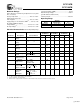
Electrical Characteristics Over the Operating Range (continued)
Parameter Description Test Conditions
7C107B-25
7C1007B-25
7C107B-35
7C1007B-35
Min. Max. Min. Max. Unit
V
OH
Output HIGH
Voltage
V
CC
= Min., I
OH
= −4.0 mA 2.4 2.4 V
V
OL
Output LOW Voltage V
CC
= Min., I
OL
= 8.0 mA 0.4 0.4 V
V
IH
Input HIGH Voltage 2.2 V
CC
+ 0.3 2.2 V
CC
+ 0.3 V
V
IL
Input LOW Voltage
[1]
−0.3 0.8 −0.3 0.8 V
I
IX
Input Load Current GND < V
I
< V
CC
−1+1−1+1µA
I
OZ
Output Leakage
Current
GND < V
I
< V
CC
,
Output Disabled
−5+5−5+5µA
I
OS
Output Short
Circuit Current
[3]
V
CC
= Max., V
OUT
= GND −300 −300 mA
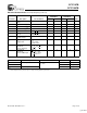
I
CC
V
CC
Operating
Supply Current
V
CC
= Max.,
I
OUT
= 0 mA,
f = f
MAX
= 1/t
RC
70 60 mA
I
SB1
Automatic CE
Power-Down
Current—TTL Inputs
Max. V
CC
, CE > V
IH
,
V
IN
>V
IH
or V
IN
< V
IL
,
f = f
MAX
20 20 mA
I
SB2
Automatic CE
Power-Down
Current—CMOS Inputs
Max. V
CC
,
CE
> V
CC
– 0.3V,
V
IN
> V
CC
– 0.3V or
V
IN
< 0.3V, f = 0
22mA
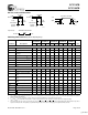
Capacitance
[4]
Parameter Description Test Conditions Max. Unit
C
IN
: Addresses Input Capacitance T
A
= 25°C, f = 1 MHz,
V
CC
= 5.0V
7pF
C
IN
: Controls 10 pF
C
OUT
Output Capacitance 10 pF
Note:
4. Tested initially and after any design or process changes that may affect these parameters.
[+] Feedback