
18-Mbit DDR-II+ SRAM 2-Word Burst Architecture (2.0 Cycle Read Latency) Specification Sheet

CY7C1146V18, CY7C1157V18
CY7C1148V18, CY7C1150V18
Document Number: 001-06621 Rev. *D Page 10 of 27
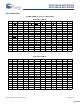
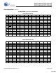
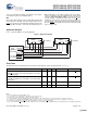
Write Cycle Descriptions
The write cycle descriptions of CY7C1146V18 and CY7C1148V18 follows.
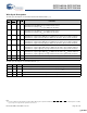
[3, 9]
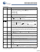
BWS
0
/
NWS
0
BWS
1
/
NWS
1
K
K
Comments
L L L – H – When the Data portion of a write sequence is active:
CY7C1146V18 − both nibbles (D
[7:0]
) are written into the device.
CY7C1148V18 − both bytes (D
[17:0]
) are written into the device.
L L – L – H When the Data portion of a write sequence is active:
CY7C1146V18 − both nibbles (D
[7:0]
) are written into the device.
CY7C1148V18 − both bytes (D
[17:0]
) are written into the device.
L H L – H – When the Data portion of a write sequence is active:
CY7C1146V18 − only the lower nibble (D
[3:0]
) is written into the device, D
[7:4]
remains unaltered.
CY7C1148V18 − only the lower byte (D
[8:0]
) is written into the device, D
[17:9]
remains unaltered.
L H – L – H When the Data portion of a write sequence is active:
CY7C1146V18 − only the lower nibble (D
[3:0]
) is written into the device, D
[7:4]
remains unaltered.
CY7C1148V18 − only the lower byte (D
[8:0]
) is written into the device, D
[17:9]
remains unaltered.
H L L – H – When the Data portion of a write sequence is active:
CY7C1146V18 − only the upper nibble (D
[7:4]
) is written into the device, D
[3:0]
remains unaltered.
CY7C1148V18 − only the upper byte (D
[17:9]
) is written into the device, D
[8:0]
remains unaltered.
H L – L – H When the Data portion of a write sequence is active:
CY7C1146V18 − only the upper nibble (D
[7:4]
) is written into the device, D
[3:0]
remains unaltered.
CY7C1148V18 − only the upper byte (D
[17:9]
) is written into the device, D
[8:0]
remains unaltered.
H H L – H – No data is written into the devices when this portion of a write operation is active.
H H – L – H No data is written into the devices when this portion of a write operation is active.
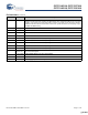
The write cycle descriptions of CY7C1146V18 follows.
[3, 9]
BWS
0
K K Comments
L L – H – When the Data portion of a write sequence is active, the single byte (D
[8:0]
) is written into the device.
L – L – H When the Data portion of a write sequence is active, the single byte (D
[8:0]
) is written into the device.
H L – H – No data is written into the device when this portion of a write operation is active.
H – L – H No data is written into the device when this portion of a write operation is active.
Note
9. Is based on a Write cycle was initiated in accordance with the Write Cycle Description Truth Table. Alter BWS
0
, BWS
1
, BWS
2
,
and BWS
3
on different portions of a Write
cycle, as long as the setup and hold requirements are achieved.
[+] Feedback [+] Feedback