
18-Mbit DDR-II+ SRAM 2-Word Burst Architecture (2.0 Cycle Read Latency) Specification Sheet

CY7C1146V18, CY7C1157V18
CY7C1148V18, CY7C1150V18
Document Number: 001-06621 Rev. *D Page 16 of 27
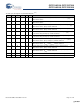
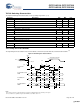
TAP AC Switching Characteristics
The Tap AC Switching Characteristics table over the operating range follows.
[14, 15]
Parameter Description Min Max Unit
t
TCYC
TCK Clock Cycle Time 50 ns
t
TF
TCK Clock Frequency 20 MHz
t
TH
TCK Clock HIGH 20 ns
t
TL
TCK Clock LOW 20 ns
Setup Times
t
TMSS
TMS Setup to TCK Clock Rise 5 ns
t
TDIS
TDI Setup to TCK Clock Rise 5 ns
t
CS
Capture Setup to TCK Rise 5 ns
Hold Times
t
TMSH
TMS Hold after TCK Clock Rise 5 ns
t
TDIH
TDI Hold after Clock Rise 5 ns
t
CH
Capture Hold after Clock Rise 5 ns
Output Times
t
TDOV
TCK Clock LOW to TDO Valid 10 ns
t
TDOX
TCK Clock LOW to TDO Invalid 0 ns
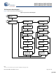
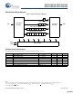
TAP Timing and Test Condition
The Tap Timing and Test Conditions for the CY7C1146V18, CY7C1157V18, CY7C1148V18, and CY7C1150V18 follows.
[15]
Figure 4. TAP Timing and Test Conditions
t
TL
t
TH
(a)
TDO
C
L
= 20 pF
Z
0
= 50
Ω
GND
0.9V
50
Ω
1.8V
0V
ALL INPUT PULSES
0.9V
Test Clock
Test Mode Select
TCK
TMS
Test Data In
TDI
Test Data Out
t
TCYC
t
TMSH
t
TMSS
t
TDIS
t
TDIH
t
TDOV
t
TDOX
TDO
Notes
14. t
CS
and t
CH
refer to the setup and hold time requirements of latching data from the boundary scan register.
15. Test conditions are specified using the load in TAP AC test conditions. t
R
/t
F
= 1 ns
[+] Feedback [+] Feedback