
18-Mbit QDRTM-II+ SRAM 4-Word Burst Architecture (2.5 Cycle Read Latency) Specification Sheet

CY7C1161V18, CY7C1176V18
CY7C1163V18, CY7C1165V18
18-Mbit QDR™-II+ SRAM 4-Word Burst
Architecture (2.5 Cycle Read Latency)
Cypress Semiconductor Corporation • 198 Champion Court • San Jose, CA 95134-1709 • 408-943-2600
Document Number: 001-06582 Rev. *D Revised March 06, 2008
Features
■ Separate independent read and write data ports
❐ Supports concurrent transactions
■ 300 MHz to 400 MHz clock for high bandwidth
■ 4-word burst to reduce address bus frequency
■ Double Data Rate (DDR) interfaces on both read and write ports
(data transferred at 800 MHz) at 400 MHz
■ Read latency of 2.5 clock cycles
■ Two input clocks (K and K) for precise DDR timing
❐ SRAM uses rising edges only
■ Echo clocks (CQ and CQ) simplify data capture in high speed
systems
■ Single multiplexed address input bus latches address inputs
for both read and write ports
■ Separate port selects for depth expansion
■ Data valid pin (QVLD) to indicate valid data on the output
■ Synchronous internally self-timed writes
■ Available in x8, x9, x18, and x36 configurations
■ Full data coherency providing most current data
■ Core V
DD
= 1.8V ± 0.1V; IO V
DDQ
= 1.4V to V
DD
[1]
■ Available in 165-ball FBGA package (13 x 15 x 1.4 mm)
■ Offered in both Pb-free and non Pb-free packages
■ Variable drive HSTL output buffers
■ JTAG 1149.1 compatible test access port
■ Delay Lock Loop (DLL) for accurate data placement
Configurations
With cycle read latency of 2.5 cycles:
CY7C1161V18 – 2M x 8
CY7C1176V18 – 2M x 9
CY7C1163V18 – 1M x 18
CY7C1165V18 – 512K x 36
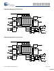
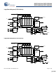
Functional Description
The CY7C1161V18, CY7C1176V18, CY7C1163V18, and
CY7C1165V18 are 1.8V Synchronous Pipelined SRAMs
equipped with QDR™-II+ architecture. QDR-II+ architecture
consists of two separate ports to access the memory array. The
read port has dedicated data outputs to support read operations
and the write port has dedicated data inputs to support write
operations. QDR-II+ architecture has separate data inputs and
data outputs to completely eliminate the need to turn around the
data bus that is required with common IO devices. Each port can
be accessed through a common address bus. Addresses for
read and write addresses are latched onto alternate rising edges
of the input (K) clock. Accesses to the QDR-II+ read and write
ports are completely independent of one another. In order to
maximize data throughput, both read and write ports are
equipped with Double Data Rate (DDR) interfaces. Each
address location is associated with four 8-bit words
(CY7C1161V18), 9-bit words (CY7C1176V18), 18-bit words
(CY7C1163V18), or 36-bit words (CY7C1165V18) that burst
sequentially into or out of the device. Because data can be trans-
ferred into and out of the device on every rising edge of both input
clocks K and K
, memory bandwidth is maximized while simpli-
fying system design by eliminating bus turnarounds.
Depth expansion is accomplished with port selects for each port.
Port selects allow each port to operate independently.
All synchronous inputs pass through input registers controlled by
the K or K
input clocks. All data outputs pass through output
registers controlled by the or K or K
input clocks. Writes are
conducted with on-chip synchronous self-timed write circuitry.
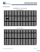
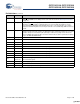
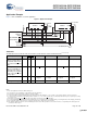
Selection Guide
Description 400 MHz 375 MHz 333 MHz 300 MHz Unit
Maximum Operating Frequency 400 375 333 300 MHz
Maximum Operating Current 1080 1020 920 850 mA
Note
1. The QDR consortium specification for V
DDQ
is 1.5V + 0.1V. The Cypress QDR devices exceed the QDR consortium specification and are capable of supporting V
DDQ
= 1.4V to V
DD
.
[+] Feedback [+] Feedback