
18-Mbit QDRTM-II+ SRAM 4-Word Burst Architecture (2.5 Cycle Read Latency) Specification Sheet

CY7C1161V18, CY7C1176V18
CY7C1163V18, CY7C1165V18
Document Number: 001-06582 Rev. *D Page 12 of 29
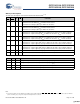
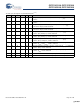
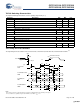
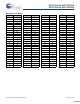
The write cycle descriptions of CY7C1165V18 follows.
[3, 11]
BWS
0
BWS
1
BWS
2
BWS
3
K K Comments
LLLLL–H–During the data portion of a write sequence, all four bytes (D
[35:0]
) are written into
the device.
LLLL–L–HDuring the data portion of a write sequence, all four bytes (D
[35:0]
) are written into
the device.
L H H H L–H – During the data portion of a write sequence, only the lower byte (D
[8:0]
) is written
into the device. D
[35:9]
remains unaltered.
L H H H – L–H During the data portion of a write sequence, only the lower byte (D
[8:0]
) is written
into the device. D
[35:9]
remains unaltered.
H L H H L–H – During the data portion of a write sequence, only the byte (D
[17:9]
) is written into
the device. D
[8:0]
and D
[35:18]
remains unaltered.
H L H H – L–H During the data portion of a write sequence, only the byte (D
[17:9]
) is written into
the device. D
[8:0]
and D
[35:18]
remains unaltered.
H H L H L–H – During the data portion of a write sequence, only the byte (D
[26:18]
) is written into
the device. D
[17:0]
and D
[35:27]
remains unaltered.
H H L H – L–H During the data portion of a write sequence, only the byte (D
[26:18]
) is written into
the device. D
[17:0]
and D
[35:27]
remains unaltered.
H H H L L–H – During the data portion of a write sequence, only the byte (D
[35:27]
) is written into
the device. D
[26:0]
remains unaltered.
H H H L – L–H During the data portion of a write sequence, only the byte (D
[35:27]
) is written into
the device. D
[26:0]
remains unaltered.
HHHHL–H–No data is written into the device during this portion of a write operation.
HHHH–L–HNo data is written into the device during this portion of a write operation.
[+] Feedback [+] Feedback