
18-Mbit Burst of 2 Pipelined SRAM with QDRTM Architecture Specification Sheet


18-Mbit Burst of 2 Pipelined SRAM with
Q
DR™ Ar
c
hi
tectu
r
e
CY7C1306BV25
CY7C1303BV25
Cypress Semiconductor Corporation • 198 Champion Court • San Jose, CA 95134-1709 • 408-943-2600
Document #: 38-05627 Rev. *A Revised April 3, 2006
Features
• Separate independent Read and Write data ports
— Supports concurrent transactions
• 167-MHz Clock for high bandwidth
— 2.5 ns Clock-to-Valid access time
• 2-Word Burst on all accesses
• Double Data Rate (DDR) interfaces on both Read and
Write Ports (data transferred at 333 MHz) @167 MHz
• Two input clocks (K and K
) for precise DDR timing
— SRAM uses rising edges only
• Two input clocks for output data (C and C
) to minimize
clock-skew and flight-time mismatches.
• Single multiplexed address input bus latches address
inputs for both Read and Write ports
• Separate Port Selects for depth expansion
• Synchronous internally self-timed writes
• 2.5V core power supply with HSTL Inputs and Outputs
• Available in 165-ball FBGA package (13 x 15 x 1.4 mm)
• Variable drive HSTL output buffers
• Expanded HSTL output voltage (1.4V–1.9V)
• JTAG Interface
• Variable Impedance HSTL
Configurations
CY7C1303BV25 – 1M x 18
CY7C1306BV25 – 512K x 36
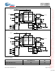
Functional Description
The CY7C1303BV25 and CY7C1306BV25 are 2.5V
Synchronous Pipelined SRAMs equipped with QDR™ archi-
tecture. QDR architecture consists of two separate ports to
access the memory array. The Read port has dedicated Data
Outputs to support Read operations and the Write Port has
dedicated Data inputs to support Write operations. Access to
each port is accomplished through a common address bus.
The Read address is latched on the rising edge of the K clock
and the Write address is latched on the rising edge of K
clock.
QDR has separate data inputs and data outputs to completely
eliminate the need to “turn-around” the data bus required with
common I/O devices. Accesses to the CY7C1303BV25/
CY7C1306BV25 Read and Write ports are completely
independent of one another. All accesses are initiated
synchronously on the rising edge of the positive input clock
(K). In order to maximize data throughput, both Read and
Write ports are equipped with Double Data Rate (DDR) inter-
faces. Therefore, data can be transferred into the device on
every rising edge of both input clocks (K and K
) and out of the
device on every rising edge of the output clock (C and C
, or K
and K
when in single clock mode) thereby maximizing perfor-
mance while simplifying system design. Each address location
is associated with two 18-bit words (CY7C1303BV25) or two
36-bit words (CY7C1306BV25) that burst sequentially into or
out of the device.
Depth expansion is accomplished with a Port Select input for
each port. Each Port Selects allow each port to operate
independently.
All synchronous inputs pass through input registers controlled
by the K or K
input clocks. All data outputs pass through output
registers controlled by the C or C
input clocks. Writes are
conducted with on-chip synchronous self-timed write circuitry.
[+] Feedback