
DDR-II SRAM 2-Word Burst Architecture Specification Sheet


CY7C1316BV18, CY7C1916BV18
CY7C1318BV18, CY7C1320BV18
Document Number: 38-05621 Rev. *D Page 15 of 31
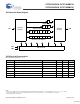
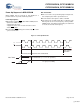
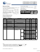
TAP Controller Block Diagram
TAP Electrical Characteristics
Over the Operating Range
[10, 11, 12]
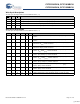
Parameter Description Test Conditions Min Max Unit
V
OH1
Output HIGH Voltage I
OH
= −2.0 mA 1.4 V
V
OH2
Output HIGH Voltage I
OH
= −100 μA1.6 V
V
OL1
Output LOW Voltage I
OL
= 2.0 mA 0.4 V
V
OL2
Output LOW Voltage I
OL
= 100 μA0.2V
V
IH
Input HIGH Voltage 0.65V
DD
V
DD
+ 0.3 V
V
IL
Input LOW Voltage –0.3 0.35V
DD
V
I
X
Input and Output Load Current GND ≤ V
I
≤ V
DD
–5 5 μA
0
012..29
3031
Boundary Scan Register
Identification Register
012..
.
.106
012
Instruction Register
Bypass Register
Selection
Circuitry
Selection
Circuitry
TAP Controller
TDI
TDO
TCK
TMS
Notes
10. These characteristics pertain to the TAP inputs (TMS, TCK, TDI and TDO). Parallel load levels are specified in the Electrical Characteristics Table.
11. Overshoot: V
IH
(AC) < V
DDQ
+ 0.85V (Pulse width less than t
CYC
/2), Undershoot: V
IL
(AC) > −1.5V (Pulse width less than t
CYC
/2).
12. All Voltage referenced to Ground.
[+] Feedback