
DDR-II SRAM 2-Word Burst Architecture Specification Sheet


CY7C1316BV18, CY7C1916BV18
CY7C1318BV18, CY7C1320BV18
Document Number: 38-05621 Rev. *D Page 6 of 31
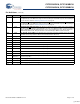
Pin Definitions
Pin Name IO Pin Description
DQ
[x:0]
Input Output-
Synchronous
Data Input Output Signals. Inputs are sampled on the rising edge of K and K clocks during valid write
operations. These pins drive out the requested data during a read operation. Valid data is driven out on
the rising edge of both the C and C
clocks during read operations or K and K when in single clock mode.
When read access is deselected, Q
[x:0]
are automatically tri-stated.
CY7C1316BV18 − DQ
[7:0]
CY7C1916BV18 − DQ
[8:0]
CY7C1318BV18 − DQ
[17:0]
CY7C1320BV18 − DQ
[35:0]
LD Input-
Synchronous
Synchronous Load. This input is brought LOW when a bus cycle sequence is defined. This definition
includes address and read/write direction. All transactions operate on a burst of 2 data.
NWS
0
,
NWS
1
Input-
Synchronous
Nibble Write Select 0, 1 − Active LOW (CY7C1316BV18 only). Sampled on the rising edge of the K
and K
clocks during write operations. Used to select which nibble is written into the device during the
current portion of the write operations. Nibbles not written remain unaltered.
NWS
0
controls D
[3:0]
and NWS
1
controls D
[7:4]
.
All the Nibble Write Selects are sampled on the same edge as the data. Deselecting a Nibble Write Select
ignores the corresponding nibble of data and it is not written into the device.
BWS
0
,
BWS
1
,
BWS
2
,
BWS
3
Input-
Synchronous
Byte Write Select 0, 1, 2, and 3 − Active LOW. Sampled on the rising edge of the K and K clocks during
write operations. Used to select which byte is written into the device during the current portion of the Write
operations. Bytes not written remain unaltered.
CY7C1916BV18 − BWS
0
controls D
[8:0]
CY7C1318BV18 − BWS
0
controls D
[8:0]
and BWS
1
controls D
[17:9].
CY7C1320BV18 − BWS
0
controls D
[8:0]
, BWS
1
controls D
[17:9]
, BWS
2
controls D
[26:18]
and BWS
3
controls
D
[35:27]
.
All the Byte Write Selects are sampled on the same edge as the data. Deselecting a Byte Write Select
ignores the corresponding byte of data and it is not written into the device.
A, A0 Input-
Synchronous
Address Inputs. These address inputs are multiplexed for both read and write operations. Internally, the
device is organized as 2M x 8 (2 arrays each of 1M x 8) for CY7C1316BV18 and 2M x 9 (2 arrays each
of 1M x 9) for CY7C1916BV18, a single 1M x 18 array for CY7C1916BV18, and a single array of 512K x
36 for CY7C1318BV18.
CY7C1316BV18 – Because the least significant bit of the address internally is a ‘0’, only 20 external
address inputs are needed to access the entire memory array.
CY7C1916BV18 – Because the least significant bit of the address internally is a ‘0’, only 20 external
address inputs are needed to access the entire memory array.
CY7C1318BV18 – A0 is the input to the burst counter. These are incremented internally in a linear fashion.
20 address inputs are needed to access the entire memory array.
CY7C1320BV18 – A0 is the input to the burst counter. These are incremented internally in a linear fashion.
19 address inputs are needed to access the entire memory array. All the address inputs are ignored when
the appropriate port is deselected.
R/W Input-
Synchronous
Synchronous Read/Write Input. When LD is LOW, this input designates the access type (read when
R/W
is HIGH, write when R/W is LOW) for the loaded address. R/W must meet the setup and hold times
around the edge of K.
C Input Clock Positive Input Clock for Output Data.
C is used in conjunction with C
to clock out the read data from
the device. C and C
can be used together to deskew the flight times of various devices on the board back
to the controller. See Application Example on page 9 for more information.
C
Input Clock Negative Input Clock for Output Data. C is used in conjunction with C to clock out the read data from
the device. C and C
can be used together to deskew the flight times of various devices on the board back
to the controller. See Application Example on page 9 for more information.
K Input Clock Positive Input Clock Input. The rising edge of K is used to capture synchronous inputs to the device
and to drive out data through Q
[x:0]
when in single clock mode. All accesses are initiated on the rising
edge of K.
K
Input Clock Negative Input Clock Input. K is used to capture synchronous data being presented to the device and
to drive out data through Q
[x:0]
when in single clock mode.
[+] Feedback