
Static RAM Datasheet


CY7C1318CV18
CY7C1320CV18
Document Number: 001-07160 Rev. *F Page 20 of 26
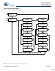
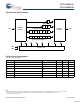
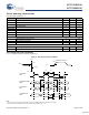
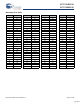
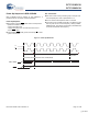
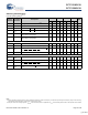
Switching Characteristics
Over the Operating Range
[20, 21]
Cypress
Parameter
Consortium
Parameter
Description
267 MHz 250 MHz 200 MHz 167 MHz
Unit
Min Max Min Max Min Max Min Max
t
POWER
V
DD
(Typical) to the First Access
[22]
1–1–1–1–ms
t
CYC
t
KHKH
K Clock and C Clock Cycle Time 3.75 8.4 4.0 8.4 5.0 8.4 6.0 8.4 ns
t
KH
t
KHKL
Input Clock (K/K and C/C) HIGH 1.5 – 1.6 – 2.0 – 2.4 – ns
t
KL
t
KLKH
Input Clock (K/K and C/C) LOW 1.5 – 1.6 – 2.0 – 2.4 – ns
t
KHKH
t
KHKH
K Clock Rise to K Clock Rise and C to C Rise
(rising edge to rising edge)
1.68 – 1.8 – 2.2 – 2.7 – ns
t
KHCH
t
KHCH
K/K Clock Rise to C/C Clock Rise
(rising edge to rising edge)
0.00 1.68 0.00 1.8 0.00 2.2 0.00 2.7 ns
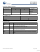
Setup Times
t
SA
t
AVKH
Address Setup to K Clock Rise 0.3 – 0.5 – 0.6 – 0.7 – ns
t
SC
t
IVKH
Control Setup to K Clock Rise (LD, R/W) 0.3 – 0.5 – 0.6 – 0.7 – ns
t
SCDDR
t
IVKH
Double Data Rate Control Setup to Clock (K/K)
Rise (BWS
0
, BWS
1
, BWS
2
, BWS
3
)
0.3 – 0.35 – 0.4 – 0.5 – ns
t
SD
t
DVKH
D
[X:0]
Setup to Clock (K and K) Rise 0.3 – 0.35 – 0.4 – 0.5 – ns
Hold Times
t
HA
t
KHAX
Address Hold after K Clock Rise 0.3 – 0.5 – 0.6 – 0.7 – ns
t
HC
t
KHIX
Control Hold after K Clock Rise (LD, R/W) 0.3 – 0.5 – 0.6 – 0.7 – ns
t
HCDDR
t
KHIX
Double Data Rate Control Hold after Clock (K/K)
Rise (BWS
0
, BWS
1
, BWS
2
, BWS
3
)
0.3 – 0.35 – 0.4 – 0.5 – ns
t
HD
t
KHDX
D
[X:0]
Hold after Clock (K/K) Rise 0.3 – 0.35 – 0.4 – 0.5 – ns
Notes
21. When a part with a maximum frequency above 167 MHz is operating at a lower clock frequency, it requires the input timings of the frequency range in which it is being
operated and outputs data with the output timings of that frequency range.
22. This part has an internal voltage regulator; t
POWER
is the time that the power is supplied above V
DD
minimum initially before a read or write operation can be initiated.
[+] Feedback