
4-Mbit (128K x 36) Pipelined SRAM with NoBLTM Architecture Specification Sheet

4-Mbit (128K x 36) Pipelined SRAM
with NoBL™ Architecture
CY7C1350G
Cypress Semiconductor Corporation • 198 Champion Court • San Jose, CA 95134-1709 • 408-943-2600
Document #: 38-05524 Rev. *F Revised July 5, 2006
Features
• Pin compatible and functionally equivalent to ZBT™
devices
• Internally self-timed output buffer control to eliminate
the need to use OE
• Byte Write capability
• 128K x 36 common I/O architecture
• 3.3V power supply (V
DD
)
• 2.5V/3.3V I/O power supply (V
DDQ
)
• Fast clock-to-output times
— 2.6 ns (for 250-MHz device)
• Clock Enable (CEN
) pin to suspend operation
• Synchronous self-timed writes
• Asynchronous output enable (OE
)
• Available in lead-free 100-Pin TQFP package, lead-free
and non-lead-free 119-Ball BGA package
• Burst Capability—linear or interleaved burst order
• “ZZ” Sleep mode option
Functional Description
[1]
The CY7C1350G is a 3.3V, 128K x 36 synchronous-pipelined
Burst SRAM designed specifically to support unlimited true
back-to-back Read/Write operations without the insertion of
wait states. The CY7C1350G is equipped with the advanced
No Bus Latency™ (NoBL™) logic required to enable consec-
utive Read/Write operations with data being transferred on
every clock cycle. This feature dramatically improves the
throughput of the SRAM, especially in systems that require
frequent Write/Read transitions.
All synchronous inputs pass through input registers controlled
by the rising edge of the clock. All data outputs pass through
output registers controlled by the rising edge of the clock. The
clock input is qualified by the Clock Enable (CEN
) signal,
which, when deasserted, suspends operation and extends the
previous clock cycle. Maximum access delay from the clock
rise is 2.6 ns (250-MHz device)
Write operations are controlled by the four Byte Write Select
(BW
[A:D]
) and a Write Enable (WE) input. All writes are
conducted with on-chip synchronous self-timed write circuitry.
Three synchronous Chip Enables (CE
1
, CE
2
, CE
3
) and an
asynchronous Output Enable (OE
) provide for easy bank
selection and output tri-state control. In order to avoid bus
contention, the output drivers are synchronously tri-stated
during the data portion of a write sequence.
Note:
1. For best-practices recommendations, please refer to the Cypress application note System Design Guidelines on www.cypress.com.
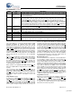
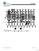
A0, A1, A
C
MODE
BW
A
BW
B
WE
CE1
CE2
CE3
OE
READ LOGIC
DQs
DQP
A
DQP
B
DQP
C
DQP
D
D
A
T
A
S
T
E
E
R
I
N
G
O
U
T
P
U
T
B
U
F
F
E
R
S
MEMORY
ARRAY
E
E
INPUT
REGISTER 0
ADDRESS
REGISTER 0
WRITE ADDRESS
REGISTER 1
WRITE ADDRESS
REGISTER 2
WRITE REGISTRY
AND DATA COHERENCY
CONTROL LOGIC
BURST
LOGIC
A0'
A1'
D1
D0
Q1
Q0
A0
A1
C
ADV/LD
ADV/LD
E
INPUT
REGISTER 1
S
E
N
S
E
A
M
P
S
E
CLK
C
EN
WRITE
DRIVERS
BW
C
BW
D
ZZ
SLEEP
CONTROL
O
U
T
P
U
T
R
E
G
I
S
T
E
R
S
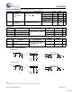
L
og
i
c
Bl
oc
k
Di
agram
[+] Feedback