
Pipelined SRAM Specification Sheet

CY7C1354CV25
CY7C1356CV25
Document #: 38-05537 Rev. *H Page 13 of 28
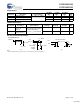
2.5V TAP AC Test Conditions
Input pulse levels ............................................... V
SS
to 2.5V
Input rise and fall time .................................................... 1 ns
Input timing reference levels ........................................1.25V
Output reference levels ................................................1.25V
Test load termination supply voltage.............................1.25V
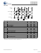
2.5V TAP AC Output Load Equivalent
T
DO
1.25V
20p
F
Z = 50Ω
O
50Ω
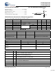
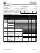
TAP DC Electrical Characteristics And Operating Conditions
(0°C < TA < +70°C; VDD = 2.5V ±0.125V unless otherwise noted)
[13]
Parameter Description Test Conditions Min. Max. Unit
V
OH1
Output HIGH Voltage I
OH
= –1.0 mA, V
DDQ
= 2.5V 2.0 V
V
OH2
Output HIGH Voltage I
OH
= –100 µA,V
DDQ
= 2.5V 2.1 V
V
OL1
Output LOW Voltage I
OL
= 8.0 mA, V
DDQ
= 2.5V 0.4 V
V
OL2
Output LOW Voltage I
OL
= 100 µA V
DDQ
= 2.5V 0.2 V
V
IH
Input HIGH Voltage V
DDQ
= 2.5V 1.7 V
DD
+ 0.3 V
V
IL
Input LOW Voltage V
DDQ
= 2.5V –0.3 0.7 V
I
X
Input Load Current GND < V
IN
< V
DDQ
–5 5 µA
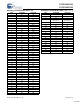
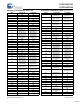
Identification Register Definitions
Instruction Field CY7C1354CV25 CY7C1356CV25 Description
Revision Number (31:29) 000 000 Reserved for version number.
Cypress Device ID (28:12) 01011001000100110 01011001000010110 Reserved for future use.
Cypress JEDEC ID (11:1) 00000110100 00000110100 Allows unique identification of SRAM vendor.
ID Register Presence (0) 1 1 Indicate the presence of an ID register.
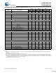
Scan Register Sizes
Register Name Bit Size (x36) Bit Size (x18)
Instruction 3 3
Bypass 1 1
ID 32 32
Boundary Scan Order (119-ball BGA
package)
69 69
Boundary Scan Order (165-ball FBGA
package)
69 69
Identification Codes
Instruction Code Description
EXTEST 000 Captures the Input/Output ring contents. Places the boundary scan register between the TDI and
TDO. Forces all SRAM outputs to High-Z state.
IDCODE 001 Loads the ID register with the vendor ID code and places the register between TDI and TDO. This
operation does not affect SRAM operation.
SAMPLE Z 010 Captures the Input/Output contents. Places the boundary scan register between TDI and TDO.
Forces all SRAM output drivers to a High-Z state.
RESERVED 011 Do Not Use: This instruction is reserved for future use.
SAMPLE/PRELOAD 100 Captures the Input/Output ring contents. Places the boundary scan register between TDI and TDO.
Does not affect the SRAM operation.
RESERVED 101 Do Not Use: This instruction is reserved for future use.
RESERVED 110 Do Not Use: This instruction is reserved for future use.
BYPASS 111 Places the bypass register between TDI and TDO. This operation does not affect SRAM operation.
Note:
13. All voltages referenced to V
SS
(GND).
[+] Feedback