
Pipelined DCD Sync SRAM Specification Sheet

CY7C1386D, CY7C1386F
CY7C1387D, CY7C1387F
Document Number: 38-05545 Rev. *E Page 10 of 30
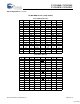
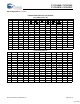
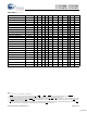
Truth Table for Read/Write
[6, 9]
Function (CY7C1386D/CY7C1386F) GW BWE BW
D
BW
C
BW
B
BW
A
Read HHXXXX
Read HLHHHH
Write Byte A – (DQ
A
and DQP
A
) HL HHHL
Write Byte B – (DQ
B
and DQP
B
)HLHHLH
Write Bytes B, A H L H H L L
Write Byte C – (DQ
C
and DQP
C
)HLHLHH
Write Bytes C, A H L H L H L
Write Bytes C, B H L H L L H
Write Bytes C, B, A H L H L L L
Write Byte D – (DQ
D
and DQP
D
)HLLHHH
Write Bytes D, A H L L H H L
Write Bytes D, B H L L H L H
Write Bytes D, B, A H L L H L L
Write Bytes D, C H L L L H H
Write Bytes D, C, A H L L L H L
Write Bytes D, C, B H L L L L H
Write All Bytes H L L L L L
Write All Bytes L X X X X X
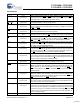
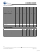
Truth Table for Read/Write
[6, 9]
Function (CY7C1387D/CY7C1387F) GW BWE BW
B
BW
A
Read HHXX
Read HLHH
Write Byte A – (DQ
A
and DQP
A
)HLHL
Write Byte B – (DQ
B
and DQP
B
)HLLH
Write All Bytes H L L L
Write All Bytes L X X X
Note
9. Table only lists a partial listing of the byte write combinations. Any Combination of BW
X
is valid Appropriate write will be done based on which byte write is active.
[+] Feedback