
Pipelined DCD Sync SRAM Specification Sheet

CY7C1386D, CY7C1386F
CY7C1387D, CY7C1387F
Document Number: 38-05545 Rev. *E Page 22 of 30
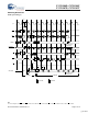
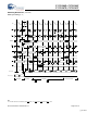
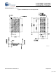
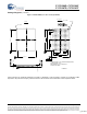
Write Cycle Timing
[26, 27]
Switching Waveforms (continued)
t
CYC
t
CL
CLK
ADSP
t
ADH
t
ADS
ADDRESS
t
CH
OE
ADSC
CE
t
AH
t
AS
A1
t
CEH
t
CES
BWE,
BW
X
ADV
BURST READ BURST WRITE
D(A2)
D(A2 + 1)
D(A3)
D(A3 + 1)
D(A2 + 3)
A2 A3
Extended BURST WRITE
Single WRITE
t
ADH
t
ADS
t
ADH
t
ADS
t
OEHZ
t
ADVH
t
ADVS
t
WEH
t
WES
t
DH
t
DS
GW
t
WEH
t
WES
Byte write signals are ignored for first cycle when
ADSP initiates burst
ADSC extends burst
ADV suspends burst
DON’T CARE UNDEFINED
D(A1)
High-Z
Data in (D)
Data Out (Q)
Note
27.
Full width write can be initiated by either GW
LOW, or by GW HIGH, BWE LOW, and BW
X
LOW.
[+] Feedback