
Dual-Port Static RAM Specification Sheet

CY7C130, CY7C130A
CY7C131, CY7C131A
CY7C140, CY7C141
Document #: 38-06002 Rev. *E Page 4 of 19
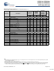
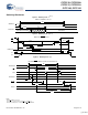
Maximum Ratings
[5]
Exceeding maximum ratings may shorten the useful life of the
device. User guidelines are not tested.
Storage Temperature ................................. –65°C to +150
°
C
Ambient Temperature with
Power Applied ............................................ –55°C to +125°C
Supply Voltage to Ground Potential
(Pin 48 to Pin 24)............................................–0.5V to +7.0V
DC Voltage Applied to Outputs
in High Z State................................................–0.5V to +7.0V
DC Input Voltage ............................................–3.5V to +7.0V
Output Current into Outputs (LOW)............................. 20 mA
Static Discharge Voltage........................................... >2001V
(per MIL-STD-883, Method 3015)
Latch Up Current .................................................... >200 mA
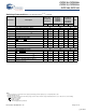
Operating Range
Range Ambient Temperature V
CC
Commercial 0
°
C to +70
°
C 5V ± 10%
Industrial –40
°
C to +85
°
C 5V ± 10%
Military
[6]
–55
°
C to +125
°
C 5V ± 10%
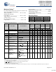
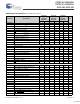
Electrical Characteristics Over the Operating Range
[7]
Parameter Description Test Conditions
7C131-15
[4]
7C131A-15
7C141-15
7C130-30
[4]
7C130A-30
7C131-25,30
7C140-30
7C141-25,30
7C130-35,45
7C131-35,45
7C140-35,45
7C141-35,45
7C130-55
7C131-55
7C140-55
7C141-55
Unit
Min Max Min Max Min Max Min Max
V
OH
Output HIGH Voltage V
CC
= Min, I
OH
= –4.0 mA 2.4 2.4 2.4 2.4 V
V
OL
Output LOW Voltage I
OL
= 4.0 mA 0.4 0.4 0.4 0.4 V
I
OL
= 16.0 mA
[8]
0.5 0.5 0.5 0.5
V
IH
Input HIGH Voltage 2.2 2.2 2.2 2.2 V
V
IL
Input LOW Voltage 0.8 0.8 0.8 0.8 V
I
IX
Input Leakage Current GND < V
I
< V
CC
–5 +5 –5 +5 –5 +5 –5 +5 μA
I
OZ
Output Leakage
Current
GND < V
O
< V
CC
,
Output Disabled
–5 +5 –5 +5 –5 +5 –5 +5 μA
I
OS
Output Short
Circuit Current
[9, 10]
V
CC
= Max,
V
OUT
= GND
–350 –350 –350 –350 mA
I
CC
V
CC
Operating
Supply Current
CE = V
IL
,
Outputs Open, f = f
MAX
[11]
Com’l 190 170 120 110 mA
I
SB1
Standby Current
Both Ports, TTL Inputs
CE
L
and CE
R
> V
IH
,
f = f
MAX
[11]
Com’l 75 65 45 35 mA
I
SB2
Standby Current
One Port,
TTL Inputs
CE
L
or CE
R
> V
IH
,
Active Port Outputs Open
f = f
MAX
[11]
Com’l 135 115 90 75 mA
I
SB3
Standby Current
Both Ports,
CMOS Inputs
Both Ports CE
L
and CE
R
>
V
CC
– 0.2V,
V
IN
> V
CC
– 0.2V
or V
IN
< 0.2V, f = 0
Com’l
15 15 15 15 mA
I
SB4
Standby Current
One Port,
CMOS Inputs
One Port CE
L
or
CE
R
> V
CC
– 0.2V,
V
IN
> V
CC
– 0.2V
or V
IN
< 0.2V,
Active Port Outputs Open, f =
f
MAX
[11]
Com’l 125 105 85 70 mA
Shaded areas contain preliminary information.
Notes
5. The voltage on any input or I/O pin cannot exceed the power pin during power up.
6. T
A
is the “instant on” case temperature
7. See the last page of this specification for Group A subgroup testing information.
8. BUSY
and INT pins only.
9. Duration of the short circuit should not exceed 30 seconds.
10. This parameter is guaranteed but not tested.
11. At f = f
MAX
, address and data inputs are cycling at the maximum frequency of read cycle of 1/t
RC
and using AC Test Waveforms input levels of GND to 3V.
[+] Feedback