
SRAM Specification Sheet


CY7C1410AV18, CY7C1425AV18
CY7C1412AV18, CY7C1414AV18
Document #: 38-05615 Rev. *E Page 9 of 29
Programmable Impedance
An external resistor, RQ, must be connected between the ZQ pin
on the SRAM and V
SS
to allow the SRAM to adjust its output
driver impedance. The value of RQ must be 5x the value of the
intended line impedance driven by the SRAM. The allowable
range of RQ to guarantee impedance matching with a tolerance
of ±15% is between 175Ω and 350Ω
, with V
DDQ
=1.5V. The
output impedance is adjusted every 1024 cycles upon power up
to account for drifts in supply voltage and temperature.
Echo Clocks
Echo clocks are provided on the QDR-II to simplify data capture
on high-speed systems. Two echo clocks are generated by the
QDR-II. CQ is referenced with respect to C and CQ
is referenced
with respect to C. These are free-running clocks and are
synchronized to the output clock (C/C
) of the QDR-II. In single
clock mode, CQ is generated with respect to K and CQ is
generated with respect to K. The timing for the echo clocks is
shown in the Switching Characteristics on page 23.
DLL
These chips use a Delay Lock Loop (DLL) that is designed to
function between 120 MHz and the specified maximum clock
frequency. During power up, when the DOFF is tied HIGH, the
DLL is locked after 1024 cycles of stable clock. The DLL can also
be reset by slowing or stopping the input clock K and K for a
minimum of 30 ns. However, it is not necessary to reset the DLL
to lock to the desired frequency. The DLL automatically locks
1024 clock cycles after a stable clock is presented. The DLL may
be disabled by applying ground to the DOFF
pin. For information
refer to the application note AN5062, DLL Considerations in
QDRII/DDRII/QDRII+/DDRII+.
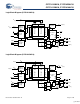
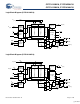
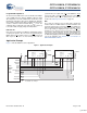
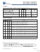
Application Example
Figure 1 shows two QDR-II used in an application.
Figure 1. Application Example
R = 250ohms
Vt
R
R = 250ohms
Vt
Vt
R
Vt = Vddq/2
R = 50ohms
R
CC#
D
A
SRAM #2
R
P
S
#
W
P
S
#
B
W
S
#
ZQ
CQ/CQ#
Q
K#
CC#
D
A
K
SRAM #1
R
P
S
#
W
P
S
#
B
W
S
#
ZQ
CQ/CQ#
Q
K#
BUS
MASTER
(CPU
or
ASIC)
DATA IN
DATA OUT
Address
RPS#
WPS#
BWS#
Source K
Source K#
Delayed K
Delayed K#
CLKIN/CLKIN#
K
[+] Feedback