
Pipelined Sync SRAM Specification Sheet

36-Mbit (1M x 36/2M x 18/512K x 72)
Pipelined Sync SRAM
CY7C1440AV33
CY7C1442AV33
CY7C1446AV33
Cypress Semiconductor Corporation • 198 Champion Court • San Jose, CA 95134-1709 • 408-943-2600
Document #: 38-05383 Rev. *E Revised June 23, 2006
Features
• Supports bus operation up to 250 MHz
• Available speed grades are 250, 200 and 167 MHz
• Registered inputs and outputs for pipelined operation
• 3.3V core power supply
• 2.5V/3.3V I/O power supply
• Fast clock-to-output times
— 2.6 ns (for 250-MHz device)
• Provide high-performance 3-1-1-1 access rate
• User-selectable burst counter supporting Intel
®
Pentium
®
interleaved or linear burst sequences
• Separate processor and controller address strobes
• Synchronous self-timed writes
• Asynchronous output enable
• Single Cycle Chip Deselect
• CY7C1440AV33, CY7C1442AV33 available in lead-free
100-pin TQFP package, lead-free and non-lead-free
165-ball FBGA package. CY7C1446AV33 available in
lead-free and non-lead-free 209-ball FBGA package
• Also available in lead-free packages
• IEEE 1149.1 JTAG-Compatible Boundary Scan
• “ZZ” Sleep Mode Option
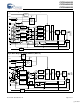
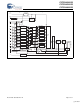
Functional Description
[1]
The CY7C1440AV33/CY7C1442AV33/CY7C1446AV33 SRAM
integrates 1M x 36/2M x 18 and 512K x 72 SRAM cells with
advanced synchronous peripheral circuitry and a two-bit
counter for internal burst operation. All synchronous inputs are
gated by registers controlled by a positive-edge-triggered
Clock Input (CLK). The synchronous inputs include all
addresses, all data inputs, address-pipelining Chip Enable
(CE
1
), depth-expansion Chip Enables (CE
2
and
CE
3
), Burst
Control inputs (ADSC
, ADSP, and ADV), Write Enables (BW
X
and BWE), and Global Write (GW). Asynchronous inputs
include the Output Enable (OE
) and the ZZ pin.
Addresses and chip enables are registered at rising edge of
clock when either Address Strobe Processor (ADSP
) or
Address Strobe Controller (ADSC
) are active. Subsequent
burst addresses can be internally generated as controlled by
the Advance pin (ADV).
Address, data inputs, and write controls are registered on-chip
to initiate a self-timed Write cycle.This part supports Byte Write
operations (see Pin Descriptions and Truth Table for further
details). Write cycles can be one to two or four bytes wide as
controlled by the byte write control inputs. GW when active
LOW
causes all bytes to be written.
The CY7C1440AV33/CY7C1442AV33/CY7C1446AV33
operates from a +3.3V core power supply while all outputs may
operate with either a +2.5 or +3.3V supply. All inputs and
outputs are JEDEC-standard JESD8-5-compatible.
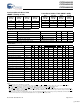
Selection Guide
250 MHz 200 MHz 167 MHz Unit
Maximum Access Time 2.6 3.2 3.4 ns
Maximum Operating Current 475 425 375 mA
Maximum CMOS Standby Current 120 120 120 mA
Note:
1. For best-practices recommendations, please refer to the Cypress application note System Design Guidelines on www.cypress.com.
[+] Feedback