
Flow-Through SRAM Specification Sheet

CY7C1471V33
CY7C1473V33
CY7C1475V33
Document #: 38-05288 Rev. *J Page 23 of 32
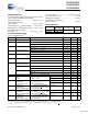
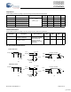
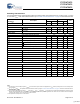
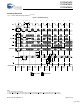
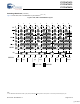
Switching Characteristics
Over the Operating Range. Unless otherwise noted in the following table, timing reference level is 1.5V when V
DDQ
= 3.3V and
is 1.25V when V
DDQ
= 2.5V. Test conditions shown in (a) of “AC Test Loads and Waveforms” on page 22 unless otherwise noted.
Parameter
Description
133 MHz 117 MHz
Unit
Min Max Min Max
t
POWER
[16]
1 1 ms
Clock
t
CYC
Clock Cycle Time 7.5 10 ns
t
CH
Clock HIGH 2.5 3.0 ns
t
CL
Clock LOW 2.5 3.0 ns
Output Times
t
CDV
Data Output Valid After CLK Rise 6.5 8.5 ns
t
DOH
Data Output Hold After CLK Rise 2.5 2.5 ns
t
CLZ
Clock to Low-Z
[17, 18, 19]
3.0 3.0 ns
t
CHZ
Clock to High-Z
[17, 18, 19]
3.8 4.5 ns
t
OEV
OE LOW to Output Valid 3.0 3.8 ns
t
OELZ
OE LOW to Output Low-Z
[17, 18, 19]
0 0 ns
t
OEHZ
OE HIGH to Output High-Z
[17, 18, 19]
3.0 4.0 ns
Setup Times
t
AS
Address Setup Before CLK Rise 1.5 1.5 ns
t
ALS
ADV/LD Setup Before CLK Rise 1.5 1.5 ns
t
WES
WE, BW
X
Setup Before CLK Rise 1.5 1.5 ns
t
CENS
CEN
Setup Before CLK Rise
1.5 1.5 ns
t
DS
Data Input Setup Before CLK Rise 1.5 1.5 ns
t
CES
Chip Enable Setup Before CLK Rise 1.5 1.5 ns
Hold Times
t
AH
Address Hold After CLK Rise 0.5 0.5 ns
t
ALH
ADV/LD Hold After CLK Rise 0.5 0.5 ns
t
WEH
WE, BW
X
Hold After CLK Rise 0.5 0.5 ns
t
CENH
CEN Hold After CLK Rise 0.5 0.5 ns
t
DH
Data Input Hold After CLK Rise 0.5 0.5 ns
t
CEH
Chip Enable Hold After CLK Rise 0.5 0.5 ns
Notes
16. This part has an internal voltage regulator; t
POWER
is the time that the power needs to be supplied above V
DD
(minimum) initially, before a read or write operation
can be initiated.
17. t
CHZ
, t
CLZ
,t
OELZ
, and t
OEHZ
are specified with AC test conditions shown in part (b) of“AC Test Loads and Waveforms” on page 22. Transition is measured ±200 mV
from steady-state voltage.
18. At any supplied voltage and temperature, t
OEHZ
is less than t
OELZ
and t
CHZ
is less than t
CLZ
to eliminate bus contention between SRAMs when sharing the same
data bus. These specifications do not imply a bus contention condition, but reflect parameters guaranteed over worst case user conditions. Device is designed
to achieve High-Z before Low-Z under the same system conditions.
19. This parameter is sampled and not 100% tested.
[+] Feedback