
Flow-Through SRAM Specification Sheet


CY7C1471V33
CY7C1473V33
CY7C1475V33
Document #: 38-05288 Rev. *J Page 31 of 32
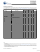
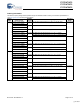
Document History Page
Document Title: CY7C1471V33/CY7C1473V33/CY7C1475V33, 72-Mbit (2M x 36/4M x 18/1M x 72) Flow-Through SRAM
with NoBL™ Architecture
Document Number: 38-05288
REV. ECN NO.
Issue
Date
Orig. of Change Description of Change
** 114675 08/06/02 PKS New Data Sheet
*A 121521 02/07/03 CJM Updated features for package offering
Updated ordering information
Changed Advanced Information to Preliminary
*B 223721 See ECN NJY Changed timing diagrams
Changed logic block diagrams
Modified Functional Description
Modified “Functional Overview” section
Added boundary scan order for all packages
Included thermal numbers and capacitance values for all packages
Removed 150-MHz speed grade offering
Included ISB and IDD values
Changed package outline for 165FBGA package and 209-Ball BGA package
Removed 119-BGA package offering
*C 235012 See ECN RYQ Minor Change: The data sheets do not match on the spec system and
external web
*D 243572 See ECN NJY Changed ball H2 from V
DD
to NC in the 165-Ball FBGA package in page 6
Modified capacitance values on page 21
*E 299511 See ECN SYT Removed 117-MHz Speed Bin
Changed Θ
JA
from 16.8 to 24.63 °C/W and Θ
JC
from 3.3 to 2.28 °C/W for 100
TQFP Package on Page # 21
Added Pb-free information for 100-Pin TQFP, 165 FBGA and 209 BGA
Packages
Added comment of ‘Pb-free BG packages availability’ below the Ordering
Information
*F 320197 See ECN PCI Corrected part number typos in the logic block diagram on page# 2
*G 331513 See ECN PCI Address expansion pins/balls in the pinouts for all packages are modified as
per JEDEC standard
Added Address Expansion pins in the Pin Definitions Table
Added Industrial Operating Range
Modified V
OL
, V
OH
Test Conditions
Updated Ordering Information Table
*H 416221 See ECN RXU Converted from Preliminary to Final
Changed address of Cypress Semiconductor Corporation on Page# 1 from
“3901 North First Street” to “198 Champion Court”
Removed 100MHz Speed bin & Added 117MHz Speed bin
Changed the description of I
X
from Input Load Current to Input Leakage
Current on page# 19
Changed the I
X
current values of MODE on page # 19 from –5 µA and 30 µA
to –30 µA and 5 µA
Changed the I
X
current values of ZZ on page # 19 from –30 µA and 5 µA
to –5 µA and 30 µA
Changed V
IH
< V
DD
to V
IH
< V
DD
on page # 19
Replaced Package Name column with Package Diagram in the Ordering
Information table
Updated the Ordering Information Table
[+] Feedback