
QDRTM-II SRAM 2-Word Burst Architecture Specification Sheet

72-Mbit QDR™-II SRAM 2-Word
Burst Architecture
CY7C1510KV18, CY7C1525KV18
CY7C1512KV18, CY7C1514KV18
Cypress Semiconductor Corporation • 198 Champion Court • San Jose, CA 95134-1709 • 408-943-2600
Document Number: 001-00436 Rev. *E Revised March 30, 2009
Features
■ Separate Independent Read and Write Data Ports
❐ Supports concurrent transactions
■ 333 MHz Clock for High Bandwidth
■ 2-word Burst on all Accesses
■ Double Data Rate (DDR) Interfaces on both Read and Write
Ports (data transferred at 666 MHz) at 333 MHz
■ Two Input Clocks (K and K) for precise DDR timing
❐ SRAM uses rising edges only
■ Two Input Clocks for Output Data (C and C) to minimize Clock
Skew and Flight Time mismatches
■ Echo Clocks (CQ and CQ) simplify Data Capture in High Speed
Systems
■ Single Multiplexed Address Input bus latches Address Inputs
for both Read and Write Ports
■ Separate Port Selects for Depth Expansion
■ Synchronous internally Self-timed Writes
■ QDR™-II operates with 1.5 Cycle Read Latency when DOFF
is asserted HIGH
■ Operates similar to QDR-I Device with 1 Cycle Read Latency
when DOFF
is asserted LOW
■ Available in x8, x9, x18, and x36 Configurations
■ Full Data Coherency, providing Most Current Data
■ Core V
DD
= 1.8V (±0.1V); IO V
DDQ
= 1.4V to V
DD
❐ Supports both 1.5V and 1.8V IO supply
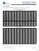
■ Available in 165-ball FBGA Package (13 x 15 x 1.4 mm)
■ Offered in both Pb-free and non Pb-free Packages
■ Variable Drive HSTL Output Buffers
■ JTAG 1149.1 Compatible Test Access Port
■ Phase Locked Loop (PLL) for Accurate Data Placement
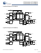
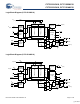
Configurations
CY7C1510KV18 – 8M x 8
CY7C1525KV18 – 8M x 9
CY7C1512KV18 – 4M x 18
CY7C1514KV18 – 2M x 36
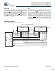
Functional Description
The CY7C1510KV18, CY7C1525KV18, CY7C1512KV18, and
CY7C1514KV18 are 1.8V Synchronous Pipelined SRAMs,
equipped with QDR-II architecture. QDR-II architecture consists
of two separate ports: the read port and the write port to access
the memory array. The read port has dedicated data outputs to
support read operations and the write port has dedicated data
inputs to support write operations. QDR-II architecture has
separate data inputs and data outputs to completely eliminate
the need to “turnaround” the data bus that exists with common
I/O devices. Access to each port is through a common address
bus. Addresses for read and write addresses are latched on
alternate rising edges of the input (K) clock. Accesses to the
QDR-II read and write ports are completely independent of one
another. To maximize data throughput, both read and write ports
are equipped with DDR interfaces. Each address location is
associated with two 8-bit words (CY7C1510KV18), 9-bit words
(CY7C1525KV18), 18-bit words (CY7C1512KV18), or 36-bit
words (CY7C1514KV18) that burst sequentially into or out of the
device. Because data can be transferred into and out of the
device on every rising edge of both input clocks (K and K
and C
and C
), memory bandwidth is maximized while simplifying
system design by eliminating bus turnarounds.
Depth expansion is accomplished with port selects, which
enables each port to operate independently.
All synchronous inputs pass through input registers controlled by
the K or K
input clocks. All data outputs pass through output
registers controlled by the C or C (or K or K in a single clock
domain) input clocks. Writes are conducted with on-chip
synchronous self-timed write circuitry.
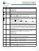
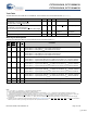
Table 1. Selection Guide
Description 333 MHz 300 MHz 250 MHz 200 MHz 167 MHz Unit
Maximum Operating Frequency 333 300 250 200 167 MHz
Maximum Operating Current x8 790 730 640 540 480 mA
x9 790 730 640 540 480
x18 810 750 650 550 490
x36 990 910 790 660 580
[+] Feedback