
QDRTM-II SRAM 2-Word Burst Architecture Specification Sheet

CY7C1510KV18, CY7C1525KV18
CY7C1512KV18, CY7C1514KV18
Document Number: 001-00436 Rev. *E Page 19 of 30
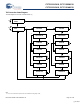
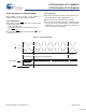
Power Up Sequence in QDR-II SRAM
QDR-II SRAMs must be powered up and initialized in a
predefined manner to prevent undefined operations.
Power Up Sequence
■ Apply power and drive DOFF either HIGH or LOW (All other
inputs can be HIGH or LOW).
❐ Apply V
DD
before V
DDQ
.
❐ Apply V
DDQ
before V
REF
or at the same time as V
REF
.
❐ Drive DOFF HIGH.
■ Provide stable DOFF (HIGH), power and clock (K, K) for 20 μs
to lock the PLL.
PLL Constraints
■ PLL uses K clock as its synchronizing input. The input must
have low phase jitter, which is specified as t
KC Var
.
■ The PLL functions at frequencies down to 120 MHz.
■ If the input clock is unstable and the PLL is enabled, then the
PLL may lock onto an incorrect frequency, causing unstable
SRAM behavior. To avoid this, provide 20 μs of stable clock to
relock to the desired clock frequency.
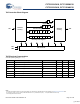
Figure 3. Power Up Waveforms
> 20Ps Stable clock
Start Normal
Operation
DOFF
Stable (< +/- 0.1V DC per 50ns )
Fix HIGH (or tie to V
DDQ
)
K
K
DDQDD
V
V
/
DDQDD
V
V
/
Clock Start
(Clock Starts after Stable)
DDQ
DD
V
V
/
~
~
~
~
Unstable Clock
[+] Feedback