
QDRTM-II SRAM 2-Word Burst Architecture Specification Sheet

CY7C1510KV18, CY7C1525KV18
CY7C1512KV18, CY7C1514KV18
Document Number: 001-00436 Rev. *E Page 6 of 30
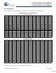
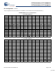
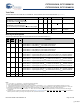
Pin Definitions
Pin Name I/O Pin Description
D
[x:0]
Input-
Synchronous
Data Input Signals. Sampled on the rising edge of K and K clocks during valid write operations.
CY7C1510KV18 − D
[7:0]
CY7C1525KV18 − D
[8:0]
CY7C1512KV18 − D
[17:0]
CY7C1514KV18 − D
[35:0]
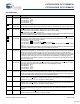
WPS Input-
Synchronous
Write Port Select − Active LOW. Sampled on the rising edge of the K clock. When asserted active, a
write operation is initiated. Deasserting deselects the write port. Deselecting the write port ignores D
[x:0]
.
NWS
0
,
NWS
1
Input-
Synchronous
Nibble Write Select 0, 1 − Active LOW (CY7C1510KV18 Only). Sampled on the rising edge of the K
and K
clocks during write operations. Used to select which nibble is written into the device during the
current portion of the write operations. Nibbles not written remain unaltered.
NWS
0
controls D
[3:0]
and NWS
1
controls D
[7:4].
All the Nibble Write Selects are sampled on the same edge as the data. Deselecting a Nibble Write Select
ignores the corresponding nibble of data and it is not written into the device.
BWS
0
,
BWS
1
,
BWS
2
,
BWS
3
Input-
Synchronous
Byte Write Select 0, 1, 2, and 3 − Active LOW. Sampled on the rising edge of the K and K clocks during
write operations. Used to select which byte is written into the device during the current portion of the write
operations. Bytes not written remain unaltered.
CY7C1525KV18 − BWS
0
controls D
[8:0].
CY7C1512KV18 − BWS
0
controls D
[8:0]
and BWS
1
controls D
[17:9].
CY7C1514KV18 − BWS
0
controls D
[8:0]
, BWS
1
controls D
[17:9]
, BWS
2
controls D
[26:18]
and BWS
3
controls
D
[35:27].
All the Byte Write Selects are sampled on the same edge as the data. Deselecting a Byte Write Select
ignores the corresponding byte of data and it is not written into the device.
A Input-
Synchronous
Address Inputs. Sampled on the rising edge of the K (read address) and K
(write address) clocks during
active read and write operations. These address inputs are multiplexed for both read and write operations.
Internally, the device is organized as 8M x 8 (2 arrays each of 4M x 8) for CY7C1510KV18, 8M x 9
(2 arrays each of 4M x 9) for CY7C1525KV18, 4M x 18 (2 arrays each of 2M x 18) for CY7C1512KV18,
and 2M x 36 (2 arrays each of 1M x 36) for CY7C1514KV18. Therefore, only 22 address inputs are needed
to access the entire memory array of CY7C1510KV18 and CY7C1525KV18, 21 address inputs for
CY7C1512KV18, and 20 address inputs for CY7C1514KV18. These inputs are ignored when the appro-
priate port is deselected.
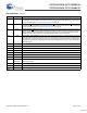
Q
[x:0]
Output-
Synchronous
Data Output Signals. These pins drive out the requested data during a read operation. Valid data is
driven out on the rising edge of the C and C
clocks during read operations, or K and K when in single
clock mode. When the read port is deselected, Q
[x:0]
are automatically tristated.
CY7C1510KV18 − Q
[7:0]
CY7C1525KV18 − Q
[8:0]
CY7C1512KV18 − Q
[17:0]
CY7C1514KV18 − Q
[35:0]
RPS Input-
Synchronous
Read Port Select − Active LOW. Sampled on the rising edge of positive input clock (K). When active, a
read operation is initiated. Deasserting deselects the read port. When deselected, the pending access is
allowed to complete and the output drivers are automatically tristated following the next rising edge of the
C clock. Each read access consists of a burst of two sequential transfers.
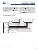
C Input Clock Positive Input Clock for Output Data. C is used in conjunction with C
to clock out the read data from
the device. Use C and C
together to deskew the flight times of various devices on the board back to the
controller. See Application Example on page 9 for further details.
C
Input Clock Negative Input Clock for Output Data. C is used in conjunction with C to clock out the read data from
the device. Use C and C
together to deskew the flight times of various devices on the board back to the
controller. See Application Example on page 9 for further details.
K Input Clock Positive Input Clock Input. The rising edge of K is used to capture synchronous inputs to the device
and to drive out data through Q
[x:0]
when in single clock mode. All accesses are initiated on the rising
edge of K.
K
Input Clock Negative Input Clock Input. K is used to capture synchronous inputs being presented to the device and
to drive out data through Q
[x:0]
when in single clock mode.
[+] Feedback