
DDR-II SRAM 2-Word Burst Architecture Specification Sheet


CY7C1516AV18, CY7C1527AV18
CY7C1518AV18, CY7C1520AV18
Document Number: 001-06982 Rev. *D Page 21 of 30
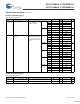
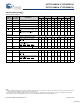
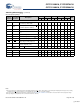
I
DD
[19]
V
DD
Operating Supply V
DD
= Max,
I
OUT
= 0 mA,
f = f
MAX
= 1/t
CYC
200MHz (x8) 700 mA
(x9) 700
(x18) 700
(x36) 735
167MHz (x8) 650 mA
(x9) 650
(x18) 650
(x36) 650
I
SB1
Automatic Power down
Current
Max V
DD
,
Both Ports Deselected,
V
IN
≥ V
IH
or V
IN
≤ V
IL
f = f
MAX
= 1/t
CYC
,
Inputs
Static
300MHz (x8) 400 mA
(x9) 400
(x18) 400
(x36) 400
278MHz (x8) 390 mA
(x9) 390
(x18) 390
(x36) 390
250MHz (x8) 380 mA
(x9) 380
(x18) 380
(x36) 380
200MHz (x8) 360 mA
(x9) 360
(x18) 360
(x36) 360
167MHz (x8) 340 mA
(x9) 340
(x18) 340
(x36) 340
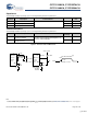
AC Electrical Characteristics
Over the Operating Range
[11]
Parameter Description Test Conditions Min Typ Max Unit
V
IH
Input HIGH Voltage V
REF
+ 0.2 – – V
V
IL
Input LOW Voltage – – V
REF
– 0.2 V
Electrical Characteristics (continued)
DC Electrical Characteristics
Over the Operating Range
[12]
Parameter Description Test Conditions Min Typ Max Unit
[+] Feedback