
Static RAM Specification Sheet

32K x 8 Static RAM
CY7C199
Cypress Semiconductor Corporation • 3901 North First Street • San Jose • CA 95134 • 408-943-2600
Document #: 38-05160 Rev. ** Revised September 7, 2001
99
Features
• High speed
—10 ns
•Fast t
DOE
• CMOS for optimum speed/power
• Low active power
— 467 mW (max, 12 ns “L” version)
• Low standby power
— 0.275 mW (max, “L” version)
• 2V data retention (“L” version only)
• Easy memory expansion with CE
and OE features
• TTL-compatible inputs and outputs
• Automatic power-down when deselected
Functional Description
The CY7C199 is a high-performance CMOS static RAM orga-
nized as 32,768 words by 8 bits. Easy memory expansion is
provided by an active LOW Chip Enable (CE
) and active LOW
Output Enable (OE
) and three-state drivers. This device has
an automatic power-down feature, reducing the power con-
sumption by 81% when deselected. The CY7C199 is in the
standard 300-mil-wide DIP, SOJ, and LCC packages.
An active LOW Write Enable signal (WE
) controls the writ-
ing/reading operation of the memory. When CE
and WE inputs
are both LOW, data on the eight data input/output pins (I/O
0
through I/O
7
) is written into the memory location addressed by
the address present on the address pins (A
0
through A
14
).
Reading the device is accomplished by selecting the device
and enabling the outputs, CE
and OE active LOW, while WE
remains inactive or HIGH. Under these conditions, the con-
tents of the location addressed by the information on address
pins are present on the eight data input/output pins.
The input/output pins remain in a high-impedance state unless
the chip is selected, outputs are enabled, and Write Enable
(WE
) is HIGH. A die coat is used to improve alpha immunity.
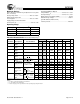
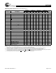
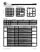
Selection Guide
7C199-8 7C199-10 7C199-12 7C199-15 7C199-20 7C199-25 7C199-35 7C199-45
Maximum Access Time (ns) 81012 15 20 25 35 45
Maximum Operating
Current (mA)
120 110 160 155 150 150 140 140
L 90 90 90 90 80 70
Maximum CMOS
Standby Current (mA)
0.5 0.5 10 10 10 10 10 10
L 0.05 0.05 0.05 0.05 0.05 0.05
Shaded area contains advance information.
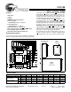
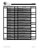
Logic Block Diagram
Pin Configurations
A
1
A
2
A
3
A
4
A
5
A
6
A
7
A
8
COLUMN
DECODER
ROW DECODER
SENSE AMPS
INPUT BUFFER
POWER
DOWN
WE
OE
I/O
0
CE
I/O
1
I/O
2
I/O
3
1
2
3
4
5
6
7
8
9
10
11
14
15
16
20
19
18
17
21
24
23
22
Top View
DIP / SOJ / SOIC
12
13
25
28
27
26
GND
A
6
A
7
A
8
A
9
A
10
A
11
A
12
A
13
WE
V
CC
A
4
A
3
A
2
A
1
I/O
7
I/O
6
I/O
5
I/O
4
A
14
A
5
I/O
0
I/O
1
I/O
2
CE
OE
A
0
I/O
3
1024 x 32 x 8
ARRAY
I/O
7
I/O
6
I/O
5
I/O
4
A
9
A
0
A
11
A
13
A
12
A
14
A
10
28
4
5
6
7
8
9
10
321 27
1314151617
26
25
24
23
22
21
20
11
12
19
18
A
7
V
CC
I/O
5
GND
WE
A
6
A
5
I/O
4
I/O
3
I/O
2
A
8
A
9
A
10
A
11
A
12
A
13
A
14
CE
A
3
A
2
A
1
A
0
I/O
1
I/O
7
I/O
6
A
4
OE
I/O
0
Top View
LCC
C199–1
C199–2
C199–3
22
23
24
25
26
27
28
1
2
5
10
11
15
14
13
12
16
19
18
17
3
4
20
21
7
6
8
9
OE
A
1
A
2
A
3
A
4
WE
V
CC
A
5
A
6
A
7
A
8
A
9
A
0
CE
I/O
7
I/O
6
I/O
5
GND
I/O
2
I/O
1
I/O
4
I/O
0
A
14
A
10
A
11
A
13
A
12
C199–4
I/O
3
TSOP I
Top View
(not to scale)