CY7C65113C USB Hub with Microcontroller USB Hub with Microcontroller Cypress Semiconductor Corporation Document #: 38-08002 Rev.
CY7C65113C TABLE OF CONTENTS 1.0 FEATURES ......................................................................................................................................5 2.0 FUNCTIONAL OVERVIEW .............................................................................................................6 3.0 PIN CONFIGURATIONS .................................................................................................................8 4.0 PRODUCT SUMMARY TABLES ..................................
CY7C65113C 16.0 USB HUB .....................................................................................................................................29 16.1 16.2 16.3 16.4 16.5 Connecting/Disconnecting a USB Device ..............................................................................29 Enabling/Disabling a USB Device ..........................................................................................30 Hub Downstream Ports Status and Control ..........................................
CY7C65113C Figure 16-5. Hub Ports Force Low Register .........................................................................................31 Figure 16-6. Hub Ports SE0 Status Register .......................................................................................31 Figure 16-7. Hub Ports Data Register ..................................................................................................32 Figure 16-8. Hub Ports Suspend Register ........................................................
CY7C65113C 1.
CY7C65113C 2.0 Functional Overview The CY7C65113C device is a one-time programmable 8-bit microcontroller with a built-in 12-Mbps USB hub that supports up to four downstream ports. The microcontroller instruction set has been optimized specifically for USB operations, although the microcontrollers can be used for a variety of non-USB embedded applications. GPIO The CY7C65113C has 11 GPIO pins (P0[7:0], P1[2:0]), both rated at 7 mA per pin (typical) sink current.
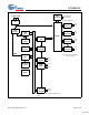
CY7C65113C Logic Block Diagram 6-MHz crystal USB Transceiver Downstream USB Ports PLL 48 MHz Clock Divider 12-MHz 8-bit CPU USB Transceiver D+[1] D–[1] USB Transceiver D+[2] D–[2] USB Transceiver D+[3] D–[3] USB Transceiver D+[4] D–[4] Repeater 12 MHz USB SIE RAM 256 byte 8-bit Bus PROM 8 KB 6 MHz D+[0] Upstream D–[0] USB Port Interrupt Controller Power management under firmware control using GPIO pins 12-bit Timer Watchdog Timer GPIO PORT 0 P0[0] GPIO PORT 1 P1[0] P0[7] P1[2]
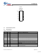
CY7C65113C 3.0 Pin Configurations Top View CY7C65113C 28-pin SOIC 4.0 4.1 XTALOUT 1 28 VCC XTALIN 2 27 P1[1] VREF 3 26 P1[0] GND 4 25 P1[2] D+[0] 5 24 D–[3] D–[0] 6 23 D+[3] D+[1] 7 22 D–[4] D–[1] 8 21 D+[4] D+[2] 9 20 GND D–[2] 10 19 VPP P0[7] 11 18 P0[0] P0[5] 12 17 P0[2] P0[3] 13 16 P0[4] P0[1] 14 15 P0[6] Product Summary Tables Pin Assignments Table 4-1.
CY7C65113C 4.2 I/O Register Summary I/O registers are accessed via the I/O Read (IORD) and I/O Write (IOWR, IOWX) instructions. IORD reads data from the selected port into the accumulator. IOWR performs the reverse; it writes data from the accumulator to the selected port. Indexed I/O Write (IOWX) adds the contents of X to the address in the instruction to form the port address and writes data from the accumulator to the specified port. Specifying address 0 (e.g.
CY7C65113C Table 4-2.
CY7C65113C Table 4-3. Instruction Set Summary (continued) MNEMONIC operand opcode cycles MNEMONIC operand opcode cycles XPAGE 1F 4 RET 3F 8 MOV A,X 40 4 DI 70 4 MOV X,A 41 4 EI 72 4 MOV PSP,A 60 4 RETI 73 8 CALL addr 50-5F 10 JC addr C0-CF 5 (or 4) JMP addr 80-8F 5 JNC addr D0-DF 5 (or 4) CALL addr 90-9F 10 JACC addr E0-EF 7 JZ addr A0-AF 5 (or 4) INDEX addr F0-FF 14 JNZ addr B0-BF 5 (or 4) 5.0 Programming Model 5.
CY7C65113C 5.1.1 Program Memory Organization after reset 14-bit PC Address 0x0000 Program execution begins here after a reset 0x0002 USB Bus Reset interrupt vector 0x0004 128-µs timer interrupt vector 0x0006 1.
CY7C65113C 5.2 8-bit Accumulator (A) The accumulator is the general-purpose register for the microcontroller. 5.3 8-bit Temporary Register (X) The “X” register is available to the firmware for temporary storage of intermediate results. The microcontroller can perform indexed operations based on the value in X. Refer to Section 5.6.3 for additional information. 5.4 8-bit Program Stack Pointer (PSP) During a reset, the Program Stack Pointer (PSP) is set to 0x00 and “grows” upward from this address.
CY7C65113C 5.5 8-bit Data Stack Pointer (DSP) The Data Stack Pointer (DSP) supports PUSH and POP instructions that use the data stack for temporary storage. A PUSH instruction pre-decrements the DSP, then writes data to the memory location addressed by the DSP. A POP instruction reads data from the memory location addressed by the DSP, then post-increments the DSP. During a reset, the DSP is reset to 0x00. A PUSH instruction when DSP equals 0x00 writes data at the top of the data RAM (address 0xFF).
CY7C65113C 6.0 Clocking XTALOUT (pin 1) XTALIN (pin 2) To Internal PLL 30 pF 30 pF Figure 6-1. Clock Oscillator On-Chip Circuit The XTALIN and XTALOUT are the clock pins to the microcontroller. The user can connect an external oscillator or a crystal to these pins. When using an external crystal, keep PCB traces between the chip leads and crystal as short as possible (less than 2 cm).
CY7C65113C 7.2 Watchdog Reset The WDR occurs when the internal Watchdog Timer rolls over. Writing any value to the write-only Watchdog Reset Clear Register (Figure 7-1) clears the timer. The timer rolls over and WDR occurs if it is not cleared within tWATCH of the last clear (see Section 23.0 for the value of tWATCH). Bit 6 of the Processor Status and Control Register (Figure 13-1) is set to record this event (the register contents are set to 010X0001 by the WDR).
CY7C65113C 9.0 General-purpose I/O Ports VCC GPIO CFG mode 2-bits OE Q2 Q1 Control Data Out Latch Internal Data Bus 14 kΩ GPIO PIN Port Write Q3* Data In Latch Port Read STRB (Latch is Transparent) Data Interrupt Latch Control Reg_Bit Interrupt Enable Interrupt Controller *Port 0,1: Low Isink Figure 9-1. Block Diagram of a GPIO Pin There are 11 GPIO pins (P0[7:0] and P1[2:0]) for the hardware interface.
CY7C65113C 9.1 GPIO Configuration Port Every GPIO port can be programmed as inputs with internal pull-ups, outputs LOW or HIGH, or Hi-Z (floating, the pin is not driven internally). In addition, the interrupt polarity for each port can be programmed. The Port Configuration bits (Figure 9-4) and the Interrupt Enable bit (Figure 9-5 through Figure 9-6) determine the interrupt polarity of the port pins .
CY7C65113C Table 9-1.
CY7C65113C Timer LSB Bit # Bit Name Read/Write Reset 7 Timer Bit 7 R 0 6 TimerBit 6 R 0 5 Timer Bit 5 R 0 4 Timer Bit 4 R 0 3 Timer Bit 3 R 0 2 Timer Bit 2 R 0 Address 0x24 1 0 Timer Bit 1 Timer Bit 0 R R 0 0 Figure 10-1. Timer LSB Register Bit [7:0]: Timer lower eight bits. Timer MSB Bit # Bit Name Read/Write Reset 7 Reserved – 0 6 Reserved – 0 5 Reserved – 0 4 Reserved – 0 3 2 Timer Bit 11 Timer Bit 10 R R 0 0 Address 0x25 0 Timer Bit 8 R 0 1 Timer Bit 9 R 0 Figure 10-2.
CY7C65113C 12.0 I2C-compatible Controller The I2C-compatible block provides a versatile two-wire communication with external devices, supporting master, slave, and multi-master modes of operation. The I2C-compatible block functions by handling the low-level signaling in hardware, and issuing interrupts as needed to allow firmware to take appropriate action during transactions. While waiting for firmware response, the hardware keeps the I2C-compatible bus idle if necessary.
CY7C65113C Table 12-1. I2C Status and Control Register Bit Definitions (continued) Bit Name Description 6 Continue/Busy Write 1 to indicate ready for next transaction. Reads 1 when I2C-compatible block is busy with a transaction, 0 when transaction is complete. 7 MSTR Mode Write to 1 for master mode, 0 for slave mode. This bit is cleared if master loses arbitration. Clearing from 1 to 0 generates Stop bit.
CY7C65113C 13.0 Processor Status and Control Register Processor Status and Control Bit # Address 0xFF 7 6 5 4 3 2 1 0 IRQ Pending Watchdog Reset USB Bus Reset Interrupt Power-on Reset Suspend Interrupt Enable Sense Reserved Run Read/Write R R/W R/W R/W R/W R R/W R/W Reset 0 0 0 1 0 0 0 1 Bit Name Figure 13-1. Processor Status and Control Register Bit 0: Run This bit is manipulated by the HALT instruction.
CY7C65113C 14.0 Interrupts Interrupts are generated by GPIO pins, internal timers, I2C-compatible operation, internal USB hub and USB traffic conditions. All interrupts are maskable by the Global Interrupt Enable Register and the USB End Point Interrupt Enable Register. Writing a ‘1’ to a bit position enables the interrupt associated with that bit position.
CY7C65113C During a reset, the contents of the Global Interrupt Enable Register and USB End Point Interrupt Enable Register are cleared, effectively disabling all interrupts, The interrupt controller contains a separate flip-flop for each interrupt. See Figure 14-3 for the logic block diagram of the interrupt controller. When an interrupt is generated, it is first registered as a pending interrupt. It stays pending until it is serviced or a reset occurs.
CY7C65113C Although Reset is not an interrupt, the first instruction executed after a reset is at PROM address 0x0000h—which corresponds to the first entry in the Interrupt Vector Table. Because the JMP instruction is two bytes long, the interrupt vectors occupy two bytes. Table 14-1. Interrupt Vector Assignments 14.
CY7C65113C 14.5 USB Endpoint Interrupts There are five USB endpoint interrupts, one per endpoint. A USB endpoint interrupt is generated after the USB host writes to a USB endpoint FIFO or after the USB controller sends a packet to the USB host. The interrupt is generated on the last packet of the transaction (e.g., on the host’s ACK on an IN transfer, or on the device ACK on an OUT transfer). If no ACK is received during an IN transaction, no interrupt is generated. 14.
CY7C65113C 3. In slave transmit mode, after the slave transmits a byte of data: The ACK bit indicates if the master that requested the byte acknowledged the byte. If more bytes are to be sent, firmware writes the next byte into the Data Register and then sets the Xmit MODE and Continue/Busy bits as required. 4. In master transmit mode, after the master sends a byte of data. Firmware should load the Data Register if necessary, and set the Xmit MODE, MSTR MODE, and Continue/Busy bits appropriately.
CY7C65113C 6. The host sends a request for the Device descriptor using the new USB address. 7. Firmware decodes the request and retrieves the Device descriptor from program memory tables. 8. The host performs a control read sequence and Firmware responds by sending its Device descriptor over the USB bus. 9. The host generates control reads from the device to request the Configuration and Report descriptors. 10.Once the device receives a Set Configuration request, its functions may now be used. 11.
CY7C65113C Hub Ports Speed Bit # 7 Bit Name Reserved Read/Write R/W Reset 0 6 Reserved R/W 0 5 Reserved R/W 0 4 Reserved R/W 0 Address 0x4A 3 2 1 0 Port 4 Speed Port 3 Speed Port 2 Speed Port 1 Speed R/W R/W R/W R/W 0 0 0 0 Figure 16-2. Hub Ports Speed Bit [0..3] : Port x Speed (where x = 1..4). Set to 1 if the device plugged in to Port x is Low Speed; Set to 0 if the device plugged in to Port x is Full Speed. Bit [4..7] : Reserved. Set to 0.
CY7C65113C The downstream USB ports are designed for connection of USB devices, but can also serve as output ports under firmware control. This allows unused USB ports to be used for functions such as driving LEDs or providing additional input signals. Pulling up these pins to voltages above VREF may cause current flow into the pin. This register is not reset by USB bus reset. These bits must be cleared before going into suspend.
CY7C65113C . Hub Ports Data Bit # 7 Bit Name Reserved Read/Write Reset 6 Reserved R 0 5 Reserved 3 Port 4 Diff. Data R R R 0 0 0 Figure 16-7. Hub Ports Data Register R 0 4 Reserved 2 Port 3 Diff. Data R 0 ADDRESS 0x50 1 0 Port 2 Diff. Port 1 Diff. Data Data R R 0 0 Bit [0..3] : Port x Diff Data (where x = 1..4). Set to 1 if D+ > D- (forced differential 1, if signal is differential, i.e. not a SE0 or SE1). Set to 0 if D- > D+ (forced differential 0, if signal is differential, i.e.
CY7C65113C Hub Ports Resume Bit # 7 Bit Name Reserved Read/Write Reset 0 6 5 4 3 2 Reserved Reserved Reserved Resume 4 Resume 3 R R 0 0 0 0 0 Figure 16-9. Hub Ports Resume Status Register Address 0x4E 1 0 Resume 2 Resume 1 R R 0 0 Bit [0..3] : Resume x (where x = 1..4). When set to 1 Port x requesting to be resumed (set by hardware); default state is 0. Bit [4..7] : Reserved. Set to 0. Resume from a selectively suspended port, with the hub not in suspend, typically involves the following actions: 1.
CY7C65113C Table 16-2. Control Bit Definition for Upstream Port Control Bits 000 Control Action Not Forcing (SIE Controls Driver) 001 Force D+[0] HIGH, D–[0] LOW 010 Force D+[0] LOW, D–[0] HIGH 011 Force SE0; D+[0] LOW, D–[0] LOW 100 Force D+[0] LOW, D–[0] LOW 101 Force D+[0] HiZ, D–[0] LOW 110 Force D+[0] LOW, D–[0] HiZ 111 Force D+[0] HiZ, D–[0] HiZ Bit 3: Bus Activity. This is a “sticky” bit that indicates if any non-idle USB event has occurred on the upstream USB port.
CY7C65113C Table 17-1.
CY7C65113C Bits[6:0] of the endpoint 0 mode register are locked from CPU write operations whenever the SIE has updated one of these bits, which the SIE does only at the end of the token phase of a transaction (SETUP... Data... ACK, OUT... Data... ACK, or IN... Data... ACK). The CPU can unlock these bits by doing a subsequent read of this register. Only endpoint 0 mode registers are locked when updated. The locking mechanism does not apply to the mode registers of other endpoints.
CY7C65113C Bit 6: Data Valid. This bit is set on receiving a proper CRC when the endpoint FIFO buffer is loaded with data during transactions. This bit is used OUT and SETUP tokens only. If the CRC is not correct, the endpoint interrupt occurs, but Data Valid is cleared to a zero. Bit 7: Data 0/1 Toggle. This bit selects the DATA packet’s toggle state: 0 for DATA0, 1 for DATA1. For IN transactions, firmware must set this bit to the desired state.
CY7C65113C 1. IN Token Host To Device S Y N C IN A D D R E N D P Device To Host C R C 5 D A T A 1/0 S Y N C Token Packet H O S T IN A D D R E N D P C R C 16 S Y N C A C K Hand Shake Packet Data Packet Host To Device S Y N C Data Host To Device UPDATE Device To Host C R C 5 S Y N C Token Packet NAK/STALL Data Packet UPDATE 2.
CY7C65113C 18.0 USB Mode Tables Table 18-1.
CY7C65113C Comments Some Mode Bits are automatically changed by the SIE in response to certain USB transactions. For example, if the Mode Bits [3:0] are set to '1111' which is ACK IN-Status OUT mode as shown in Table 18-1, the SIE will change the endpoint Mode Bits [3:0] to NAK IN-Status OUT mode (1110) after ACK’ing a valid status stage OUT token. The firmware needs to update the mode for the SIE to respond appropriately. See Table 18-1 for more details on what modes will be changed by the SIE.
CY7C65113C . Table 18-3.
CY7C65113C Table 18-3.
CY7C65113C 19.0 Register Summary Bit 7 Bit 6 Bit 5 Bit 4 Bit 3 Bit 2 Bit 1 Bit 0 Read/Write/B oth/–[7] Default/ Reset Port 0 Data P0.7 P0.6 P0.5 P0.4 P0.3 P0.2 P0.1 P0.0 BBBBBBBB 11111111 0x01 Port 1 Data P1.7 P1.6 P1.5 P1.4 P1.3 P1.2 P1.1 P1.0 BBBBBBBB 11111111 0x02 Port 2 Data P2.7 P2.6 P2.5 P2.4 P2.3 P2.2 P2.1 P2.0 BBBBBBBB 11111111 0x03 Port 3 Data P3.7 P3.6 P3.5 P3.4 P3.3 P3.2 P3.1 P3.0 BBBBBBBB 11111111 0x04 Port 0 Interrupt Enable P0.
CY7C65113C HUB PORT CONTROL, STATUS, SUSPEND RESUME, SE0, FORCE LOW HUB PORT CONTROL, STATUS, SUSPEND RESUME, SE0, FORCE LOW 19.
CY7C65113C 20.0 Sample Schematic 3.3V Regulator OUT IN GND 2.2 µF USB-A Vbus D– D+ GND Vref 2.2 µF Vref 1.5K (RUUP) USB-B Vbus D– D+ GND 0.01 µF Vbus 0.01 µF Optional D0– D0+ 22x8(Rext) Vref SHELL Vcc 22x2(Rext) D1- 4.7 nF 250 VAC D1+ D2XTALO 10M 6.000 MHz D2+ XTALI D3- GND GND Vpp D3+ D4D4+ 15K(x8) (RUDN) POWER MANAGEMENT 21.0 USB-A Vbus D– D+ GND USB-A Vbus D– D+ GND USB-A Vbus D– D+ GND Absolute Maximum Ratings Storage Temperature .........................................
CY7C65113C 22.0 Electrical Characteristics fOSC = 6 MHz; Operating Temperature = 0 to 70°C, VCC = 4.0V to 5.25V Parameter Description Conditions Min. Max. Unit 3.15 3.45 V –0.4 0.4 V 50 mA General VREF Reference Voltage Vpp Programming Voltage (disabled) ICC VCC Operating Current 3.
CY7C65113C 23.0 Switching Characteristics (fOSC = 6.0 MHz) Parameter Description Min. Max. Unit Clock Source fOSC Clock Rate 6 ±0.25% tcyc Clock Period tCH Clock HIGH time tCL Clock LOW time 166.25 MHz 167.08 ns 0.45 tCYC ns 0.45 tCYC ns USB Full-speed Signaling[10] trfs Transition Rise Time 4 20 ns tffs Transition Fall Time 4 20 ns trfmfs Rise/Fall Time Matching; (tr/tf) 90 111 tdratefs Full Speed Date Rate twatch Watchdog Timer Period 12 ±0.
CY7C65113C 24.0 Ordering Information Ordering Code PROM Size Package Type Operating Range CY7C65113C-SXC 8 KB 28-pin SOIC Commercial CY7C65113C-SXCT 8 KB 28-pin SOIC-Tape Reel Commercial 25.0 Package Diagram 28-Lead (300-Mil) Molded SOIC NOTE : PIN 1 ID 1. JEDEC STD REF MO-119 2. BODY LENGTH DIMENSION DOES NOT INCLUDE MOLD PROTRUSION/END FLASH,BUT 14 DOES INCLUDE MOLD MISMATCH AND ARE MEASURED AT THE MOLD PARTING LINE. 1 MOLD PROTRUSION/END FLASH SHALL NOT EXCEED 0.010 in (0.
CY7C65113C Document History Page Document Title: CY7C65113C USB Hub with Microcontroller Document Number: 38-08002 REV. ECN NO. Issue Date Orig. of Change ** 109965 02/22/02 SZV Change from Spec number: 38-00590 to 38-08002 *A 120372 12/17/02 MON Added register bit definitions. Added default bit state of each register. Corrected the Schematic (location of the pull-up on D+). Corrected the Logical Diagram (removed the extra GPIO Port 1). Added register summary.