
Flexible USB NAND Flash Controller Specification Sheet


CY7C68033/CY7C68034
Document #: 001-04247 Rev. *D Page 15 of 33
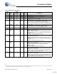
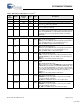
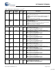
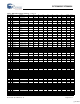
13 GPIO8 GPIO8 I/O/Z I GPIO8: is a bidirectional IO port pin.
14 Reserved# N/A Input N/A Reserved. Connect to ground.
15 SCL N/A OD Z Clock for the I
2
C interface. Connect to VCC with a 2.2K resistor,
even if no I
2
C peripheral is attached.
16 SDATA N/A OD Z Data for the I
2
C interface. Connect to VCC with a 2.2K resistor, even
if no I
2
C peripheral is attached.
44 WAKEUP Unused Input N/A USB Wakeup. If the 8051 is in suspend, asserting this pin starts up
the oscillator and interrupts the 8051 to allow it to exit the suspend
mode. Holding WAKEUP asserted inhibits the EZ-USB chip from
suspending. This pin has programmable polarity, controlled by
WAKEUP[4].
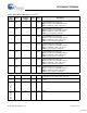
Port A
33 PA0 or
INT0#
CLE I/O/Z I
(PA0)
Multiplexed pin whose function is selected by PORTACFG[0]
PA0 is a bidirectional IO port pin.
INT0# is the active-LOW 8051 INT0 interrupt input signal, which is
either edge triggered (IT0 = 1) or level triggered (IT0 = 0).
CLE is the NAND Command Latch Enable signal.
34 PA1 or
INT1#
ALE I/O/Z I
(PA1)
Multiplexed pin whose function is selected by PORTACFG[1]
PA1 is a bidirectional IO port pin.
INT1# is the active-LOW 8051 INT1 interrupt input signal, which is
either edge triggered (IT1 = 1) or level triggered (IT1 = 0).
ALE is the NAND Address Latch Enable signal.
35 PA2 or
SLOE
LED1# I/O/Z I
(PA2)
Multiplexed pin whose function is selected by IFCONFIG[1:0].
PA2 is a bidirectional IO port pin.
SLOE is an input-only output enable with programmable polarity
(FIFOPINPOLAR[4]) for the slave FIFOs connected to FD[7:0] or
FD[15:0].
LED1# is the data activity indicator LED sink pin.
36 PA3 or
WU2
LED2# I/O/Z I
(PA3)
Multiplexed pin whose function is selected by WAKEUP[7] and
OEA[3]
PA3 is a bidirectional I/O port pin.
WU2 is an alternate source for USB Wakeup, enabled by WU2EN
bit (WAKEUP[1]) and polarity set by WU2POL (WAKEUP[4]). If the
8051 is in suspend and WU2EN = 1, a transition on this pin starts
up the oscillator and interrupts the 8051 to allow it to exit the suspend
mode. Asserting this pin inhibits the chip from suspending, if
WU2EN = 1.
LED2# is the chip activity indicator LED sink pin.
37 PA4 or
FIFOADR0
WP_NF# I/O/Z I
(PA4)
Multiplexed pin whose function is selected by IFCONFIG[1:0].
PA4 is a bidirectional I/O port pin.
FIFOADR0 is an input-only address select for the slave FIFOs
connected to FD[7:0] or FD[15:0].
WP_NF# is the NAND write-protect control output signal.
38 PA5 or
FIFOADR1
WP_SW# I/O/Z I
(PA5)
Multiplexed pin whose function is selected by IFCONFIG[1:0].
PA5 is a bidirectional I/O port pin.
FIFOADR1 is an input-only address select for the slave FIFOs
connected to FD[7:0] or FD[15:0].
WP_SW# is the NAND write-protect switch input signal.
Table 8. NX2LP-Flex Pin Descriptions (continued)
[6]
56 QFN
Pin
Number
Default Pin
Name
NAND
Firmware
Usage
Pin
Type
Default
State
Description
[+] Feedback