CY8C21634, CY8C21534 CY8C21434, CY8C21334, CY8C21234 PSoC® Programmable System-on-Chip™ Features ■ ■ Powerful Harvard Architecture Processor ❐ M8C Processor Speeds to 24 MHz ❐ Low power at high speed ❐ 2.4V to 5.25V Operating Voltage ❐ Operating Voltages Down to 1.
CY8C21634, CY8C21534 CY8C21434, CY8C21334, CY8C21234 PSoC Functional Overview The PSoC family consists of many Mixed-Signal Array with On-Chip Controller devices. These devices are designed to replace multiple traditional MCU-based system components with one low cost single-chip programmable component. A PSoC device includes configurable blocks of analog and digital logic, and programmable interconnect.
CY8C21634, CY8C21534 CY8C21434, CY8C21334, CY8C21234 The Analog System The Analog Multiplexer System The Analog System consists of 4 configurable blocks that allow the creation of complex analog signal flows. Analog peripherals are very flexible and may be customized to support specific application requirements. Some of the common PSoC analog functions for this device (most available as user modules) are: The Analog Mux Bus can connect to every GPIO pin.
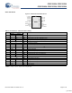
CY8C21634, CY8C21534 CY8C21434, CY8C21334, CY8C21234 PSoC Device Characteristics Depending on your PSoC device characteristics, the digital and analog systems can have 16, 8, or 4 digital blocks and 12, 6, or 4 analog blocks. Table 1 lists the resources available for specific PSoC device groups. The PSoC device covered by this data sheet is highlighted in this table.
CY8C21634, CY8C21534 CY8C21434, CY8C21334, CY8C21234 Development Tools PSoC Designer is a Microsoft® Windows-based, integrated development environment for the Programmable System-on-Chip (PSoC) devices. The PSoC Designer IDE runs on Windows XP or Windows Vista. This system provides design database management by project, an integrated debugger with In-Circuit Emulator, in-system programming support, and built-in support for third-party assemblers and C compilers.
CY8C21634, CY8C21534 CY8C21434, CY8C21334, CY8C21234 Designing with PSoC Designer The development process for the PSoC device differs from that of a traditional fixed function microprocessor. The configurable analog and digital hardware blocks give the PSoC architecture a unique flexibility that pays dividends in managing specification change during development and by lowering inventory costs.
CY8C21634, CY8C21534 CY8C21434, CY8C21334, CY8C21234 Document Conventions Units of Measure Acronyms Used A units of measure table is located in the Electrical Specifications section. Table 2 on page 7 lists all the abbreviations used to measure the PSoC devices. The following table lists the acronyms that are used in this document. Table 2.
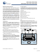
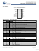
CY8C21634, CY8C21534 CY8C21434, CY8C21334, CY8C21234 Pin Information The CY8C21x34 PSoC device is available in a variety of packages which are listed in the following tables. Every port pin (labeled with a “P”) is capable of Digital IO and connection to the common analog bus. However, Vss, Vdd, SMP, and XRES are not capable of Digital IO. 16-Pin Part Pinout Figure 3.
CY8C21634, CY8C21534 CY8C21434, CY8C21334, CY8C21234 20-Pin Part Pinout Figure 4. CY8C21334 20-Pin PSoC Device A, I, M, P0[7] A, I, M, P0[5] A, I, M, P0[3] A, I, M, P0[1] Vss M,I2C SCL,P1[7] M,I2C SDA, P1[5] M,P1[3] M,I2C SCL,P1[1] Vss 1 2 3 4 5 6 7 8 9 10 SSOP 20 19 18 17 16 15 14 13 12 11 Vdd P0[6], A, I, M P0[4], A, I, M P0[2], A, I, M P0[0], A, I, M XRES P1[6],M P1[4], EXTCLK,M P1[2],M P1[0],I2C SDA, M Table 4. Pin Definitions - CY8C21334 20-Pin (SSOP) Pin No.
CY8C21634, CY8C21534 CY8C21434, CY8C21334, CY8C21234 28-Pin Part Pinout Figure 5.
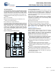
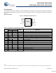
CY8C21634, CY8C21534 CY8C21434, CY8C21334, CY8C21234 32-Pin Part Pinout Figure 6. CY8C21434 32-Pin PSoC Device M, 12C SDA, P1[5] M, P1[3] M, 12C SCL, P1[1] Vss M, 12C SDA, P1[0] M, P1[2] M, EXTCLK, P1[4] M, P1[6] Document Number: 38-12025 Rev.
CY8C21634, CY8C21534 CY8C21434, CY8C21334, CY8C21234 Table 6. Pin Definitions - CY8C21434/CY8C21634 32-Pin (QFN)[4] Pin No.
CY8C21634, CY8C21534 CY8C21434, CY8C21334, CY8C21234 56-Pin Part Pinout The 56-pin SSOP part is for the CY8C21001 On-Chip Debug (OCD) PSoC device. Note This part is only used for in-circuit debugging. It is NOT available for production. Figure 12.
CY8C21634, CY8C21534 CY8C21434, CY8C21334, CY8C21234 Table 7. Pin Definitions - CY8C21001 56-Pin (SSOP) (continued) Type Pin No.
CY8C21634, CY8C21534 CY8C21434, CY8C21334, CY8C21234 Register Reference This chapter lists the registers of the CY8C21x34 PSoC device. For detailed register information, refer the PSoC Programmable System-on-Chip Technical Reference Manual. Register Conventions The register conventions specific to this section are listed in Table 8. Table 8.
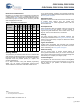
CY8C21634, CY8C21534 CY8C21434, CY8C21334, CY8C21234 DBB00DR0 DBB00DR1 DBB00DR2 DBB00CR0 DBB01DR0 DBB01DR1 DBB01DR2 DBB01CR0 DCB02DR0 DCB02DR1 DCB02DR2 DCB02CR0 DCB03DR0 DCB03DR1 DCB03DR2 DCB03CR0 20 # AMX_IN 21 W AMUXCFG 22 RW PWM_CR 23 # 24 # CMP_CR0 25 W 26 RW CMP_CR1 27 # 28 # ADC0_CR 29 W ADC1_CR 2A RW 2B # 2C # TMP_DR0 2D W TMP_DR1 2E RW TMP_DR2 2F # TMP_DR3 30 31 32 ACE00CR1 33 ACE00CR2 34 35 36 ACE01CR1 37 ACE01CR2 38 39 3A 3B 3C 3D 3E 3F Blank fields are Reserved and must not be accessed.
CY8C21634, CY8C21534 CY8C21434, CY8C21334, CY8C21234 15 16 17 18 19 1A 1B 1C 1D 1E 1F DBB00FN 20 RW CLK_CR0 DBB00IN 21 RW CLK_CR1 DBB00OU 22 RW ABF_CR0 23 AMD_CR0 DBB01FN 24 RW CMP_GO_EN DBB01IN 25 RW DBB01OU 26 RW AMD_CR1 27 ALT_CR0 DCB02FN 28 RW DCB02IN 29 RW DCB02OU 2A RW 2B CLK_CR3 DCB03FN 2C RW TMP_DR0 DCB03IN 2D RW TMP_DR1 DCB03OU 2E RW TMP_DR2 2F TMP_DR3 30 31 32 ACE00CR1 33 ACE00CR2 34 35 36 ACE01CR1 37 ACE01CR2 38 39 3A 3B 3C 3D 3E 3F Blank fields are Reserved and must not be accessed.
CY8C21634, CY8C21534 CY8C21434, CY8C21334, CY8C21234 Electrical Specifications This section presents the DC and AC electrical specifications of the CY8C21x34 PSoC device. For up to date electrical specifications, visit the web site http://www.cypress.com/psoc. Specifications are valid for -40oC ≤ TA ≤ 85oC and TJ ≤ 100oC as specified, except where noted. Refer Table 25 on page 26 for the electrical specifications on the internal main oscillator (IMO) using SLIMO mode. Figure 13.
CY8C21634, CY8C21534 CY8C21434, CY8C21334, CY8C21234 Absolute Maximum Ratings Table 12. Absolute Maximum Ratings Symbol Description TSTG Storage Temperature Min -55 Typ 25 Max +100 Units oC TA Vdd VIO Ambient Temperature with Power Applied Supply Voltage on Vdd Relative to Vss DC Input Voltage – – – DC Voltage Applied to Tri-state IMIO ESD LU Maximum Current into any Port Pin Electro Static Discharge Voltage Latch-up Current – – – +85 +6.0 Vdd + 0.5 Vdd + 0.5 +50 – 200 oC VIOZ -40 -0.5 Vss 0.
CY8C21634, CY8C21534 CY8C21434, CY8C21334, CY8C21234 Table 14. DC Chip-Level Specifications (continued) Symbol Description Min Typ Max Units Notes ISB27 Sleep (Mode) Current with POR, LVD, Sleep Timer, WDT, and internal slow oscillator active. Mid temperature range. – 2.6 4. μA Vdd = 2.55V, 0oC ≤ TA ≤ 40oC. ISB Sleep (Mode) Current with POR, LVD, Sleep Timer, WDT, and internal slow oscillator active. – 2.8 5 μA Vdd = 3.3V, -40oC ≤ TA ≤ 85oC. VREF Reference Voltage (Bandgap) 1.28 1.
CY8C21634, CY8C21534 CY8C21434, CY8C21334, CY8C21234 Table 16. 2.7V DC GPIO Specifications (continued) Symbol Description Min Typ Max Units Notes VIH Input High Level 2.0 – – V VH Input Hysteresis – 90 – mV IIL Input Leakage (Absolute Value) – 1 – nA Gross tested to 1 μA. CIN Capacitive Load on Pins as Input – 3.5 10 pF Package and pin dependent. Temp = 25oC. COUT Capacitive Load on Pins as Output – 3.5 10 pF Package and pin dependent. Temp = 25oC. Vdd = 2.4 to 3.0.
CY8C21634, CY8C21534 CY8C21434, CY8C21334, CY8C21234 Table 19. 2.7V DC Operational Amplifier Specifications Symbol Min Typ Max Units – 2.5 15 mV TCVOSOA Average Input Offset Voltage Drift – 10 – μV/oC IEBOA[5] Input Leakage Current (Port 0 Analog Pins) – 200 – pA Gross tested to 1 μA. CINOA Input Capacitance (Port 0 Analog Pins) – 4.5 9.5 pF Package and pin dependent. Temp = 25oC.
CY8C21634, CY8C21534 CY8C21434, CY8C21334, CY8C21234 Table 21. DC Switch Mode Pump (SMP) Specifications (continued) Symbol Description ΔVPUMP_ Line Regulation (over Vi range) Min Typ Max Units Notes – 5 – %VO Configuration of footnote.[6] VO is the “Vdd Value for PUMP Trip” specified by the VM[2:0] setting in the DC POR and LVD Specification, Table 23 on page 24. – 5 – %VO Configuration of footnote.
CY8C21634, CY8C21534 CY8C21434, CY8C21334, CY8C21234 DC Analog Mux Bus Specifications Table 22 lists the guaranteed maximum and minimum specifications for the voltage and temperature ranges: 4.75V to 5.25V and -40°C ≤ TA ≤ 85°C, 3.0V to 3.6V and -40°C ≤ TA ≤ 85°C, or 2.4V to 3.0V and -40°C ≤ TA ≤ 85°C, respectively. Typical parameters apply to 5V, 3.3V, or 2.7V at 25°C and are for design guidance only. Table 22.
CY8C21634, CY8C21534 CY8C21434, CY8C21334, CY8C21234 DC Programming Specifications Table 24 lists the guaranteed maximum and minimum specifications for the voltage and temperature ranges: 4.75V to 5.25V and -40°C ≤ TA ≤ 85°C, 3.0V to 3.6V and -40°C ≤ TA ≤ 85°C, or 2.4V to 3.0V and -40°C ≤ TA ≤ 85°C, respectively. Typical parameters apply to 5V, 3.3V, or 2.7V at 25°C and are for design guidance only. Table 24.
CY8C21634, CY8C21534 CY8C21434, CY8C21334, CY8C21234 AC Electrical Characteristics AC Chip-Level Specifications The following tables list the guaranteed maximum and minimum specifications for the voltage and temperature ranges: 4.75V to 5.25V and -40°C ≤ TA ≤ 85°C, 3.0V to 3.6V and -40°C ≤ TA ≤ 85°C, or 2.4V to 3.0V and -40°C ≤ TA ≤ 85°C, respectively. Typical parameters apply to 5V, 3.3V, or 2.7V at 25°C and are for design guidance only. Table 25. 5V and 3.
CY8C21634, CY8C21534 CY8C21434, CY8C21334, CY8C21234 Table 26. 2.7V AC Chip-Level Specifications Symbol FIMO12 Description Internal Main Oscillator Frequency for 12 MHz Min 11.5 Typ 120 Max 12.7[16,17,18] Units MHz FIMO6 Internal Main Oscillator Frequency for 6 MHz 5.75 6 6.35[16,17,18] MHz FCPU1 CPU Frequency (2.7V Nominal) 0.093 3 3.15[16,17] MHz FBLK27 Digital PSoC Block Frequency (2.7V Nominal) 0 12 12.
CY8C21634, CY8C21534 CY8C21434, CY8C21334, CY8C21234 AC General Purpose IO Specifications The following tables list the guaranteed maximum and minimum specifications for the voltage and temperature ranges: 4.75V to 5.25V and -40°C ≤ TA ≤ 85°C, 3.0V to 3.6V and -40°C ≤ TA ≤ 85°C, or 2.4V to 3.0V and -40°C ≤ TA ≤ 85°C, respectively. Typical parameters apply to 5V, 3.3V, or 2.7V at 25°C and are for design guidance only. Table 27. 5V and 3.
CY8C21634, CY8C21534 CY8C21434, CY8C21334, CY8C21234 AC Analog Mux Bus Specifications Table 31 lists the guaranteed maximum and minimum specifications for the voltage and temperature ranges: 4.75V to 5.25V and -40°C ≤ TA ≤ 85°C, 3.0V to 3.6V and -40°C ≤ TA ≤ 85°C, or 2.4V to 3.0V and -40°C ≤ TA ≤ 85°C, respectively. Typical parameters apply to 5V, 3.3V, or 2.7V at 25°C and are for design guidance only. Table 31. AC Analog Mux Bus Specifications Symbol FSW Description Switch Rate Min – Typ – Max 3.
CY8C21634, CY8C21534 CY8C21434, CY8C21334, CY8C21234 Table 33. 2.7V AC Digital Block Specifications Function Description All Functions Maximum Block Clocking Frequency Timer Capture Pulse Width Maximum Frequency, With or Without Capture Counter Enable Pulse Width Min Typ Max Units 12.7 MHz 100[20] – – ns – – 12.7 MHz 100 – – ns Maximum Frequency, No Enable Input – – 12.7 MHz Maximum Frequency, Enable Input – – 12.
CY8C21634, CY8C21534 CY8C21434, CY8C21334, CY8C21234 Table 35. 3.3V AC External Clock Specifications Symbol Description Min Typ Max Units Notes FOSCEXT Frequency with CPU Clock divide by 1 0.093 – 12.3 MHz Maximum CPU frequency is 12 MHz at 3.3V. With the CPU clock divider set to 1, the external clock must adhere to the maximum frequency and duty cycle requirements. FOSCEXT Frequency with CPU Clock divide by 2 or greater 0.186 – 24.
CY8C21634, CY8C21534 CY8C21434, CY8C21334, CY8C21234 Table 37. AC Programming Specifications (continued) Symbol TWRITE TDSCLK TDSCLK3 TDSCLK2 Description Flash Block Write Time Data Out Delay from Falling Edge of SCLK Data Out Delay from Falling Edge of SCLK Data Out Delay from Falling Edge of SCLK Min – – – – Typ 30 – – – Max – 45 50 70 Units ms ns ns ns Notes 3.6 < Vdd 3.0 ≤ Vdd ≤ 3.6 2.4 ≤ Vdd ≤ 3.
CY8C21634, CY8C21534 CY8C21434, CY8C21334, CY8C21234 Table 39. 2.7V AC Characteristics of the I2C SDA and SCL Pins (Fast Mode not Supported) Symbol Description FSCLI2C THDSTAI2C SCL Clock Frequency Hold Time (repeated) START Condition. After this period, the first clock pulse is generated.
CY8C21634, CY8C21534 CY8C21434, CY8C21334, CY8C21234 Packaging Information This section shows the packaging specifications for the CY8C21x34 PSoC device with the thermal impedances for each package. Important Note Emulation tools may require a larger area on the target PCB than the chip’s footprint. For a detailed description of the emulation tools’ dimensions, refer to the document titled PSoC Emulator Pod Dimensions at http://www.cypress.com/design/MR10161. Packaging Dimensions Figure 20.
CY8C21634, CY8C21534 CY8C21434, CY8C21334, CY8C21234 Figure 22. 28-Pin (210-Mil) SSOP 51-85079 *C Figure 23. 32-Pin (5x5 mm 0.93 MAX) QFN E-PAD X, Y for this product is 3.53 mm, 3.53 mm (+/-0.11 mm) 51-85188 *B Document Number: 38-12025 Rev.
CY8C21634, CY8C21534 CY8C21434, CY8C21334, CY8C21234 Figure 24. 32-Pin (5x5 mm 0.60 MAX) QFN E-PAD X, Y for this product is 3.53 mm, 3.53 mm (+/-0.11 mm) 001-06392 *A Figure 25. 32-Pin (5 X 5 X 0.4MM) QFN (SAWN 1.85 X 2.85 EPAD 001-44368 *A Document Number: 38-12025 Rev.
CY8C21634, CY8C21534 CY8C21434, CY8C21334, CY8C21234 Figure 26. 32-Pin Sawn QFN Package 001-30999 *A Figure 27. 32-Pin Thin Sawn QFN Package 001-42168 *C Important Note For information on the preferred dimensions for mounting QFN packages, see the following Application Note at http://www.amkor.com/products/notes_papers/MLFAppNote.pdf. Document Number: 38-12025 Rev.
CY8C21634, CY8C21534 CY8C21434, CY8C21334, CY8C21234 Figure 28. 56-Pin (300-Mil) SSOP 51-85062 *C Thermal Impedances Table 40. Thermal Impedances per Package Package 16 SOIC 20 SSOP 28 SSOP 32 QFN[23] 5x5 mm 0.60 MAX 32 QFN[23] 5x5 mm 0.93 MAX Document Number: 38-12025 Rev.
CY8C21634, CY8C21534 CY8C21434, CY8C21334, CY8C21234 Solder Reflow Peak Temperature Following is the minimum solder reflow peak temperature to achieve good solderability. Table 41. Solder Reflow Peak Temperature Minimum Peak Temperature[24] Maximum Peak Temperature 16 SOIC 240oC 260oC 20 SSOP 240oC 260oC 28 SSOP 240oC 260oC 32 QFN 240oC 260oC Package Notes 22. TJ = TA + Power x θJA 23.
CY8C21634, CY8C21534 CY8C21434, CY8C21334, CY8C21234 Development Tool Selection ■ 110 ~ 240V Power Supply, Euro-Plug Adapter ■ iMAGEcraft C Compiler (Registration Required) ■ ISSP Cable Software ■ USB 2.0 Cable and Blue Cat-5 Cable PSoC Designer™ ■ 2 CY8C29466-24PXI 28-PDIP Chip Samples At the core of the PSoC development software suite is PSoC Designer. Used by thousands of PSoC developers, this robust software has been facilitating PSoC designs for half a decade.
CY8C21634, CY8C21534 CY8C21434, CY8C21334, CY8C21234 CY3210-PSoCEval1 Device Programmers The CY3210-PSoCEval1 kit features an evaluation board and the MiniProg1 programming unit. The evaluation board includes an LCD module, potentiometer, LEDs, and plenty of breadboarding space to meet all of your evaluation needs. The kit includes: All device programmers can be purchased from the Cypress Online Store.
CY8C21634, CY8C21534 CY8C21434, CY8C21334, CY8C21234 Temperature Range Digital IO Pins Analog Inputsa Analog Outputs XRES Pin 8K 512 Yes -40°C to +85°C 4 4 12 12[27] 0 No 16 Pin (150-Mil) SOIC (Tape and Reel) CY8C21234-24SXIT 8K 512 Yes -40°C to +85°C 4 4 12 12[27] 0 No 20 Pin (210-Mil) SSOP CY8C21334-24PVXI 8K 512 No -40°C to +85°C 4 4 16 16[27] 0 Yes 20 Pin (210-Mil) SSOP (Tape and Reel) CY8C21334-24PVXIT 8K 512 No -40°C to +85°C 4 4 16 16[27] 0 Yes 28 P
CY8C21634, CY8C21534 CY8C21434, CY8C21334, CY8C21234 Ordering Code Definitions CY 8 C 21 xxx-24xx Package Type: Thermal Rating: PX = PDIP Pb-Free C = Commercial SX = SOIC Pb-Free I = Industrial PVX = SSOP Pb-Free E = Extended LFX/LKX = QFN Pb-Free AX = TQFP Pb-Free Speed: 24 MHz Part Number Family Code Technology Code: C = CMOS Marketing Code: 8 = Cypress PSoC Company ID: CY = Cypress Document Number: 38-12025 Rev.
CY8C21634, CY8C21534 CY8C21434, CY8C21334, CY8C21234 Document History Page Document Title: CY8C21234/CY8C21334/CY8C21434/CY8C21534/CY8C21634 PSoC® Programmable System-on-Chip™ Document Number: 38-12025 Revision ECN No. Orig. of Change Submission Date Description of Change ** 227340 HMT See ECN New silicon and document (Revision **). *A 235992 SFV See ECN Updated Overview and Electrical Spec. chapters, along with revisions to the 24-pin pinout part. Revised the register mapping tables.
CY8C21634, CY8C21534 CY8C21434, CY8C21334, CY8C21234 Sales, Solutions, and Legal Information Worldwide Sales and Design Support Cypress maintains a worldwide network of offices, solution centers, manufacturer’s representatives, and distributors. To find the office closest to you, visit us at cypress.com/sales. Products PSoC Clocks & Buffers PSoC Solutions psoc.cypress.com clocks.cypress.com General Low Power/Low Voltage psoc.cypress.com/solutions psoc.cypress.com/low-power Wireless wireless.cypress.