
PSoC Programmable System-on-Chip Specification Sheet


CY8C21634, CY8C21534
CY8C21434, CY8C21334, CY8C21234
Document Number: 38-12025 Rev. *O Page 31 of 45
AC Programming Specifications
Tab le 3 7 lists the guaranteed maximum and minimum specifications for the voltage and temperature ranges: 4.75V to 5.25V and -40°C
≤ T
A
≤ 85°C, or 3.0V to 3.6V and -40°C ≤ T
A
≤ 85°C, respectively. Typical parameters apply to 5V, 3.3V, or 2.7V at 25°C and are for
design guidance only.
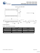
Table 35. 3.3V AC External Clock Specifications
Symbol Description Min Typ Max Units Notes
F
OSCEXT
Frequency with CPU Clock divide by 1 0.093 – 12.3 MHz Maximum CPU frequency is 12
MHz at 3.3V. With the CPU clock
divider set to 1, the external clock
must adhere to the maximum
frequency and duty cycle
requirements.
F
OSCEXT
Frequency with CPU Clock divide by 2 or
greater
0.186 – 24.6 MHz If the frequency of the external clock
is greater than 12 MHz, the CPU
clock divider must be set to 2 or
greater. In this case, the CPU clock
divider ensures that the fifty percent
duty cycle requirement is met.
– High Period with CPU Clock divide by 1 41.7
– 5300 ns
– Low Period with CPU Clock divide by 1 41.7
– –ns
– Power Up IMO to Switch 150
– – μs
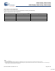
Table 36. 2.7V AC External Clock Specifications
Symbol Description Min Typ Max Units Notes
F
OSCEXT
Frequency with CPU Clock divide by 1 0.093 –3.08
0
MHz Maximum CPU frequency is 3 MHz
at 2.7V. With the CPU clock divider
set to 1, the external clock must
adhere to the maximum frequency
and duty cycle requirements.
F
OSCEXT
Frequency with CPU Clock divide by 2 or
greater
0.186 – 6.35 MHz If the frequency of the external clock
is greater than 3 MHz, the CPU
clock divider must be set to 2 or
greater. In this case, the CPU clock
divider ensures that the fifty percent
duty cycle requirement is met.
– High Period with CPU Clock divide by 1 160
– 5300 ns
– Low Period with CPU Clock divide by 1 160 – –ns
– Power Up IMO to Switch 150
– – μs
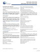
Table 37. AC Programming Specifications
Symbol Description Min Typ Max Units Notes
T
RSCLK
Rise Time of SCLK 1 – 20 ns
T
FSCLK
Fall Time of SCLK 1 – 20 ns
T
SSCLK
Data Set up Time to Falling Edge of SCLK 40 – – ns
T
HSCLK
Data Hold Time from Falling Edge of SCLK 40 – – ns
F
SCLK
Frequency of SCLK 0 – 8 MHz
T
ERASEB
Flash Erase Time (Block) – 15 – ms
[+] Feedback