CY8C23433, CY8C23533 PSoC® Programmable System-on-Chip™ Features ■ Powerful Harvard Architecture Processor ❐ M8C Processor Speeds to 24 MHz ❐ 8x8 Multiply, 32-Bit Accumulate ❐ Low Power at High Speed ❐ 3.0 to 5.
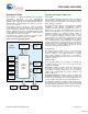
CY8C23433, CY8C23533 PSoC Functional Overview Digital System The PSoC family consists of many mixed-signal array with On-Chip Controller devices. These devices are designed to replace multiple traditional MCU-based system components with a low cost single-chip programmable device. PSoC devices include configurable blocks of analog and digital logic, and programmable interconnects.
CY8C23433, CY8C23533 The Analog system consists of an 8-bit SAR ADC and four configurable blocks. The programmable 8-bit SAR ADC is an optimized ADC that runs up to 300 Ksps, with monotonic guarantee. It also has the features to support a motor control application. Each analog block consists of an opamp circuit allowing the creation of complex analog signal flows. Analog peripherals are very flexible and can be customized to support specific application requirements.
CY8C23433, CY8C23533 Getting Started Additional System Resources System Resources, some of which are listed in the previous sections, provide additional capability useful to complete systems. Additional resources include a multiplier, decimator, low voltage detection, and power on reset. Brief statements describing the merits of each system resource follow: ■ ■ Digital clock dividers provide three customizable clock frequencies for use in applications.
CY8C23433, CY8C23533 Development Tools PSoC Designer Software Subsystems PSoC Designer is a Microsoft® Windows-based, integrated development environment for the Programmable System-on-Chip (PSoC) devices. The PSoC Designer IDE and application runs on Windows NT 4.0, Windows 2000, Windows Millennium (Me), or Windows XP (refer section PSoC Designer Subsystems on page 5).
CY8C23433, CY8C23533 Debugger The PSoC Designer Debugger subsystem provides hardware in-circuit emulation, allowing the designer to test the program in a physical system while providing an internal view of the PSoC device. Debugger commands allow the designer to read and program and read and write data memory, read and write IO registers, read and write CPU registers, set and clear breakpoints, and provide program run, halt, and step control.
CY8C23433, CY8C23533 The next step is to write your main program, and any sub-routines using PSoC Designer’s Application Editor subsystem. The Application Editor includes a Project Manager that allows you to open the project source code files (including all generated code files) from a hierarchal view. The source code editor provides syntax coloring and advanced edit features for both C and assembly language. File search capabilities include simple string searches and recursive “grep-style” patterns.
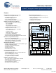
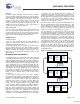
CY8C23433, CY8C23533 Pinouts The PSoC CY8C23X33 is available in 32-pin QFN and 28-pin SSOP packages. Every port pin (labeled with a “P”), except for Vss and Vdd in the following table and figure, is capable of Digital IO. 32-Pin Part Pinout Table 3.
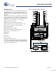
CY8C23433, CY8C23533 28-Pin Part Pinout IO 2 IO I IO Figure 6. CY8C23433 28-Pin PSoC Device Pin Name Digital 1 Analog Pin Number CY8C23433 Table 4.
CY8C23433, CY8C23533 Register Reference Register Mapping Tables This section lists the registers of the CY8C23433 PSoC device by using mapping tables, in offset order. Register Conventions Abbreviations Used The register conventions specific to this section are listed in the following table. The PSoC device has a total register address space of 512 bytes. The register space is referred to as IO space and is divided into two banks.
CY8C23433, CY8C23533 DBB00DR0 DBB00DR1 DBB00DR2 DBB00CR0 DBB01DR0 DBB01DR1 DBB01DR2 DBB01CR0 DCB02DR0 DCB02DR1 DCB02DR2 DCB02CR0 DCB03DR0 DCB03DR1 DCB03DR2 DCB03CR0 Gray fields are reserved.
CY8C23433, CY8C23533 Gray fields are reserved. CPU_SCR1 CPU_SCR0 Access BE BF Name Access Addr (0,Hex) Name Access 7E 7F Addr (0,Hex) 3E 3F Addr (0,Hex) Name Access Addr (0,Hex) Name Table 6. Register Map Bank 0 Table: User Space (continued) FE FF # # # Access is bit specific. DBB00FN DBB00IN DBB00OU DBB01FN DBB01IN DBB01OU DCB02FN DCB02IN DCB02OU DCB03FN DCB03IN DCB03OU Gray fields are reserved.
CY8C23433, CY8C23533 Gray fields are reserved. FLS_PR1 F5 F6 F7 F8 F9 FA FB FC FD FE FF CPU_F CPU_SCR1 CPU_SCR0 Access RW RW Addr (1,Hex) B5 B6 B7 B8 B9 BA BB BC BD BE BF Name RDI0RO0 RDI0RO1 Access RW RW RW Addr (1,Hex) 75 76 77 78 79 7A 7B 7C 7D 7E 7F Name Access Name ACB01CR0 ACB01CR1 ACB01CR2 * Addr (1,Hex) 35 36 37 38 39 3A 3B 3C 3D 3E 3F Access Addr (1,Hex) Name Table 7. Register Map Bank 1 Table: Configuration Space (continued) RL RW # # # Access is bit specific.
CY8C23433, CY8C23533 Electrical Specifications This section presents the DC and AC electrical specifications of the CY8C23433 PSoC device. For the latest electrical specifications, visit http://www.cypress.com/psoc. Specifications are valid for -40°C ≤ TA ≤ 85°C and TJ ≤ 100°C, except where noted. Refer to Table 24 on page 25 for the electrical specifications on the internal main oscillator (IMO) using SLIMO mode. Figure 7. Voltage versus CPU Frequency 5.25 SLIMO Mode = 0 Figure 8.
CY8C23433, CY8C23533 Absolute Maximum Ratings Exceeding maximum ratings may shorten the useful life of the device. User guidelines are not tested. Table 9. Absolute Maximum Ratings Symbol Description Min Typ Max Units -55 25 +100 °C Ambient Temperature with Power Applied -40 – +85 °C Supply Voltage on Vdd Relative to Vss -0.5 – +6.0 V DC Input Voltage Vss - 0.5 – Vdd + 0.5 V DC Voltage Applied to Tri-state Vss - 0.5 – Vdd + 0.
CY8C23433, CY8C23533 DC Electrical Characteristics DC Chip-Level Specifications The following table lists the guaranteed maximum and minimum specifications for the voltage and temperature ranges: 4.75V to 5.25V and -40°C ≤ TA ≤ 85°C, or 3.0V to 3.6V and -40°C ≤ TA ≤ 85°C, respectively. Typical parameters apply to 5V and 3.3V at 25°C and are for design guidance only. Table 11. DC Chip-Level Specifications Symbol Description Vdd Supply Voltage Min 3.0 Typ – Max 5.
CY8C23433, CY8C23533 DC General Purpose IO Specifications The following table lists the guaranteed maximum and minimum specifications for the voltage and temperature ranges: 4.75V to 5.25V and -40°C ≤ TA ≤ 85°C, or 3.0V to 3.6V and -40°C ≤ TA ≤ 85°C, respectively. Typical parameters apply to 5V and 3.3V at 25°C and are for design guidance only. Table 12. 5V and 3.3V DC GPIO Specifications Symbol Description Min Typ Max Units Notes RPU Pull up Resistor 4 5.6 8 kΩ RPD Pull down Resistor 4 5.
CY8C23433, CY8C23533 DC Operational Amplifier Specifications The following table lists the guaranteed maximum and minimum specifications for the voltage and temperature ranges: 4.75V to 5.25V and -40°C ≤ TA ≤ 85°C, or 3.0V to 3.6V and -40°C ≤ TA ≤ 85°C, respectively. Typical parameters apply to 5V and 3.3V at 25°C and are for design guidance only. The Operational Amplifier is a component of both the Analog Continuous Time PSoC blocks and the Analog Switched Cap PSoC blocks.
CY8C23433, CY8C23533 Table 14. 3.3V DC Operational Amplifier Specifications Symbol VOSOA Description Input Offset Voltage (absolute value) Power = Low, Opamp Bias = High Power = Medium, Opamp Bias = High High Power is 5 Volts Only TCVOSOA Average Input Offset Voltage Drift Min Typ Max Units – – 1.65 1.32 10 8 mV mV – 7.0 35.0 μV/°C Notes IEBOA Input Leakage Current (Port 0 Analog Pins) – 20 – pA Gross tested to 1 μA. CINOA Input Capacitance (Port 0 Analog Pins) – 4.5 9.
CY8C23433, CY8C23533 DC Analog Output Buffer Specifications The following table lists the guaranteed maximum and minimum specifications for the voltage and temperature ranges: 4.75V to 5.25V and -40°C ≤ TA ≤ 85°C, or 3.0V to 3.6V and -40°C ≤ TA ≤ 85°C, respectively. Typical parameters apply to 5V and 3.3V at 25°C and are for design guidance only. Table 16.
CY8C23433, CY8C23533 DC Analog Reference Specifications The following table lists the guaranteed maximum and minimum specifications for the voltage and temperature ranges: 4.75V to 5.25V and -40°C ≤ TA ≤ 85°C, or 3.0V to 3.6V and -40°C ≤ TA ≤ 85°C, respectively. Typical parameters apply to 5V and 3.3V at 25°C and are for design guidance only. The guaranteed specifications are measured through the Analog Continuous Time PSoC blocks.
CY8C23433, CY8C23533 Table 19. 3.3V DC Analog Reference Specifications (continued) Symbol Description Min Typ – RefHi = 2 x BandGap + P2[6] (P2[6] = 0.5V) – RefHi = P2[4] + BandGap (P2[4] = Vdd/2) – RefHi = P2[4] + P2[6] (P2[4] = Vdd/2, P2[6] = 0.5V) – RefHi = 3.2 x BandGap Not Allowed – RefLo = Vdd/2 - BandGap Not Allowed – RefLo = BandGap Not Allowed – RefLo = 2 x BandGap - P2[6] (P2[6] = 0.
CY8C23433, CY8C23533 DC Programming Specifications The following table lists the guaranteed maximum and minimum specifications for the voltage and temperature ranges: 4.75V to 5.25V and -40°C ≤ TA ≤ 85°C, or 3.0V to 3.6V and -40°C ≤ TA ≤ 85°C, respectively. Typical parameters apply to 5V and 3.3V at 25°C and are for design guidance only. Table 22. DC Programming Specifications Symbol Description VddIWRITE Supply Voltage for Flash Write Operations Min Typ Max Units Notes 2.
CY8C23433, CY8C23533 SAR8 ADC DC Specifications The following table lists the guaranteed maximum and minimum specifications for the voltage and temperature ranges: 4.75V to 5.25V and -40°C ≤ TA ≤ 85°C, or 3.0V to 3.6V and -40°C ≤ TA ≤ 85°C, respectively. Typical parameters apply to 5V and 3.3V at 25°C and are for design guidance only. Table 23.
CY8C23433, CY8C23533 AC Electrical Characteristics AC Chip-Level Specifications The following table lists the guaranteed maximum and minimum specifications for the voltage and temperature ranges: 4.75V to 5.25V and -40°C ≤ TA ≤ 85°C, or 3.0V to 3.6V and -40°C ≤ TA ≤ 85°C, respectively. Typical parameters apply to 5V and 3.3V at 25°C and are for design guidance only. Table 24. 5V and 3.3V AC Chip-Level Specifications Min Typ Max FIMO24 Symbol Internal Main Oscillator Frequency for 24 MHz 23.4 24 24.
CY8C23433, CY8C23533 Figure 9. PLL Lock Timing Diagram PLL Enable TPLLSLEW 24 MHz FPLL PLL Gain 0 Figure 10. PLL Lock for Low Gain Setting Timing Diagram PLL Enable TPLLSLEWLOW 24 MHz FPLL PLL Gain 1 Figure 11. External Crystal Oscillator Startup Timing Diagram 32K Select 32 kHz TOS F32K2 Figure 12. 24 MHz Period Jitter (IMO) Timing Diagram Jitter24M1 F 24M Figure 13. 32 kHz Period Jitter (ECO) Timing Diagram Jitter32k F 32K2 Document Number: 001-44369 Rev.
CY8C23433, CY8C23533 AC General Purpose IO Specifications The following table lists the guaranteed maximum and minimum specifications for the voltage and temperature ranges: 4.75V to 5.25V and -40°C ≤ TA ≤ 85°C, or 3.0V to 3.6V and -40°C ≤ TA ≤ 85°C, respectively. Typical parameters apply to 5V and 3.3V at 25°C and are for design guidance only. Table 25. 5V and 3.3V AC GPIO Specifications Symbol Description Min Typ Max Units Notes FGPIO GPIO Operating Frequency 0 – 12.
CY8C23433, CY8C23533 Table 27. 3.3V AC Operational Amplifier Specifications Symbol TROA TSOA SRROA SRFOA BWOA Description Rising Settling Time from 80% of ΔV to 0.1% of ΔV (10 pF load, Unity Gain) Power = Low, Opamp Bias = Low Power = Medium, Opamp Bias = High Falling Settling Time from 20% of ΔV to 0.
CY8C23433, CY8C23533 When bypassed by a capacitor on P2[4], the noise of the analog ground signal distributed to each block is reduced by a factor of up to 5 (14 dB). This is at frequencies above the corner frequency defined by the on-chip 8.1k resistance and the external capacitor. Figure 15. Typical AGND Noise with P2[4] Bypass dBV/rtHz 10000 0 0.01 0.1 1.0 10 1000 100 0.001 0.01 0.
CY8C23433, CY8C23533 AC Low Power Comparator Specifications The following table lists the guaranteed maximum and minimum specifications for the voltage and temperature ranges: 4.75V to 5.25V and -40°C ≤ TA ≤ 85°C, or 3.0V to 3.6V and -40°C ≤ TA ≤ 85°C, respectively. Typical parameters apply to 5V and 3.3V at 25°C and are for design guidance only. Table 28.
CY8C23433, CY8C23533 AC Analog Output Buffer Specifications The following table lists the guaranteed maximum and minimum specifications for the voltage and temperature ranges: 4.75V to 5.25V and -40°C ≤ TA ≤ 85°C, or 3.0V to 3.6V and -40°C ≤ TA ≤ 85°C, respectively. Typical parameters apply to 5V and 3.3V at 25°C and are for design guidance only. Table 30. 5V AC Analog Output Buffer Specifications Symbol Description Min Typ Max Units TROB Rising Settling Time to 0.
CY8C23433, CY8C23533 AC External Clock Specifications The following table lists the guaranteed maximum and minimum specifications for the voltage and temperature ranges: 4.75V to 5.25V and -40°C ≤ TA ≤ 85°C, or 3.0V to 3.6V and -40°C ≤ TA ≤ 85°C, respectively. Typical parameters apply to 5V and 3.3V at 25°C and are for design guidance only. Table 32. 5V AC External Clock Specifications Symbol Description Min Typ Max Units FOSCEXT Frequency 0.093 – 24.6 MHz – High Period 20.
CY8C23433, CY8C23533 AC I2C Specifications The following table lists the guaranteed maximum and minimum specifications for the voltage and temperature ranges: 4.75V to 5.25V and -40°C ≤ TA ≤ 85°C, or 3.0V to 3.6V and -40°C ≤ TA ≤ 85°C, respectively. Typical parameters apply to 5V and 3.3V at 25°C and are for design guidance only. Table 36. AC Characteristics of the I2C SDA and SCL Pins for Vdd > 3.
CY8C23433, CY8C23533 Packaging Information This section illustrates the packaging specifications for the CY8C23x33 PSoC device, along with the thermal impedances for each package, solder reflow peak temperature, and the typical package capacitance on crystal pins. Figure 19. 32-Pin (5x5 mm) QFN SEE NOTE 1 TOP VIEW BOTTOM VIEW SIDE VIEW NOTES: 1. HATCH AREA IS SOLDERABLE EXPOSED PAD CYPRESS COMPANY CONFIDENTIAL 2. BASED ON REF JEDEC # MO-248 3. PACKAGE WEIGHT: 0.0388g 4.
CY8C23433, CY8C23533 Figure 20. 28-Pin (210-Mil) SSOP 51-85079 *C Thermal Impedances Capacitance on Crystal Pins Table 38. Thermal Impedances by Package Table 39. Typical Package Capacitance on Crystal Pins Typical θJA[22] Package 32 QFN 28 SSOP Package Package Capacitance 19.4°C/W 32 QFN 2.0 pF 95°C/W 28 SSOP 2.8 pF Solder Reflow Peak Temperature Following is the minimum solder reflow peak temperature to achieve good solderability. Table 40.
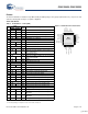
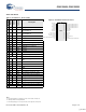
CY8C23433, CY8C23533 Ordering Information The following table lists the CY8C23X33 PSoC device family key package features and ordering codes. Document Number: 001-44369 Rev.
CY8C23433, CY8C23533 Document History Page Document Title: CY8C23433, CY8C23533 PSoC® Programmable System-on-Chip™ Document Number: 001-44369 Revision ECN Orig. of Change Submission Date Description of Change ** 2044848 KIY/AESA 01/30/2008 Data sheet creation *A 2482967 HMI/AESA 05/14/2008 Moved from Preliminary to Final. Part number changed to CY8C23433, CY8C23533.