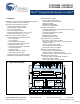
CY8C24094, CY8C24794 CY8C24894, CY8C24994 PSoC® Programmable System-on-Chip™ 1. Features ■ XRES Pin to Support In-System Serial Programming (ISSP) and External Reset Control in CY8C24894 ■ Powerful Harvard Architecture Processor ❐ M8C Processor Speeds to 24 MHz ❐ Two 8x8 Multiply, 32-Bit Accumulate ❐ Low Power at High Speed ❐ 3V to 5.
CY8C24094, CY8C24794 CY8C24894, CY8C24994 The PSoC family consists of many Mixed-Signal Array with On-Chip Controller devices. All PSoC family devices are designed to replace traditional MCUs, system ICs, and the numerous discrete components that surround them. The PSoC CY8C24x94 devices are unique members of the PSoC family because it includes a full featured, full speed (12 Mbps) USB port.
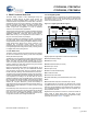
CY8C24094, CY8C24794 CY8C24894, CY8C24994 Figure 3-2. Analog System Block Diagram The Analog System is composed of 6 configurable blocks, each comprised of an opamp circuit allowing the creation of complex analog signal flows. Analog peripherals are very flexible and can be customized to support specific application requirements. Some of the more common PSoC analog functions (most available as user modules) are listed below.
CY8C24094, CY8C24794 CY8C24894, CY8C24994 4. Getting Started 3.1 Additional System Resources System Resources, provide additional capability useful to complete systems. Additional resources include a multiplier, decimator, low voltage detection, and power on reset. Brief statements describing the merits of each resource follow. ■ Full-Speed USB (12 Mbps) with 5 configurable endpoints and 256 bytes of RAM. No external components required except two series resistors.
CY8C24094, CY8C24794 CY8C24894, CY8C24994 5. Development Tools PSoC Designer is a Microsoft® Windows-based, integrated development environment for the Programmable System-on-Chip (PSoC) devices. The PSoC Designer IDE runs on Windows XP or Windows Vista. This system provides design database management by project, an integrated debugger with In-Circuit Emulator, in-system programming support, and built-in support for third-party assemblers and C compilers.
CY8C24094, CY8C24794 CY8C24894, CY8C24994 6. Designing with PSoC Designer The development process for the PSoC device differs from that of a traditional fixed function microprocessor. The configurable analog and digital hardware blocks give the PSoC architecture a unique flexibility that pays dividends in managing specification change during development and by lowering inventory costs.
CY8C24094, CY8C24794 CY8C24894, CY8C24994 7. Document Conventions 7.2 Units of Measure 7.1 Acronyms Used A units of measure table is located in the Electrical Specifications section. Table 10-1 on page 20 lists all the abbreviations used to measure the PSoC devices. The following table lists the acronyms that are used in this document.
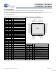
CY8C24094, CY8C24794 CY8C24894, CY8C24994 8. Pin Information This section describes, lists, and illustrates the CY8C24x94 PSoC device family pins and pinout configuration. The CY8C24x94 PSoC devices are available in the following packages, all of which are shown on the following pages. Every port pin (labeled with a “P”) is capable of Digital I/O. However, Vss, Vdd, and XRES are not capable of Digital I/O. 8.1 56-Pin Part Pinout Table 8-1.
CY8C24094, CY8C24794 CY8C24894, CY8C24994 8.1 56-Pin Part Pinout (with XRES) Table 8-2. 56-Pin Part Pinout (QFN[2]) 29 I/O M P5[0] 30 I/O M P5[2] Type Pin No. Digital Analog Name 31 I/O M P5[4] 44 I/O M P2[6] External Voltage Reference (VREF) input. 32 I/O M P5[6] 45 I/O I, M P0[0] Analog column mux input. 33 I/O M P3[0] 46 I/O I, M P0[2] Analog column mux input. 34 I/O M P3[2] 47 I/O I, M P0[4] Analog column mux input VREF.
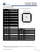
CY8C24094, CY8C24794 CY8C24894, CY8C24994 8.1 68-Pin Part Pinout The 68-pin QFN part table and drawing below is for the CY8C24994 PSoC device. Table 8-3. 68-Pin Part Pinout (QFN[2]) M M M P4[0] P4[2] P4[4] P2[6], M, Ext. VREF P2[4], M, Ext.
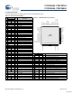
CY8C24094, CY8C24794 CY8C24894, CY8C24994 8.1 68-Pin Part Pinout (On-Chip Debug) The 68-pin QFN part table and drawing below is for the CY8C24094 On-Chip Debug (OCD) PSoC device. Note This part is only used for in-circuit debugging. It is NOT available for production. Table 8-4. 68-Pin Part Pinout (QFN[2]) Type Pin No. Digital Analog 50 I/O M I2C Serial Data (SDA), ISSP SDATA[1]. 51 I/O I,M 52 I/O I,M Optional External Clock Input (EXTCLK).
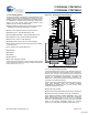
CY8C24094, CY8C24794 CY8C24894, CY8C24994 8.1 100-Ball VFBGA Part Pinout The 100-ball VFBGA part is for the CY8C24994 PSoC device.
CY8C24094, CY8C24794 CY8C24894, CY8C24994 Figure 8-5.
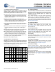
CY8C24094, CY8C24794 CY8C24894, CY8C24994 Table 8-6. 100-Ball Part Pinout (VFBGA) (continued) C8 C9 C10 D1 D2 D3 D4 D5 I/O I/O I,M M I/O I/O I/O I/O D6 D7 D8 D9 D10 E1 E2 E3 E4 E5 E6 E7 E8 E9 E10 I/O I/O I/O I/O M M M I/O, M I,M M M M I/O M I/O I,M Power Power I/O M I/O M I/O M P2[0] P4[2] NC NC P3[7] P4[5] P2[5] P0[3] Direct switched capacitor block input. H8 H9 No connection. H10 No connection. J1 J2 J3 J4 Analog column mux input and column output.
CY8C24094, CY8C24794 CY8C24894, CY8C24994 8.1 100-Pin Part Pinout (On-Chip Debug) The 100-pin TQFP part is for the CY8C24094 On-Chip Debug (OCD) PSoC device. Note This part is only used for in-circuit debugging. It is NOT available for production.
CY8C24094, CY8C24794 CY8C24894, CY8C24994 Table 8-7. 100-Pin Part Pinout (TQFP) (continued) LEGENDA = Analog, I = Input, O = Output, NC = No Connection, M = Analog Mux Input, OCD = On-Chip Debugger. Document Number: 38-12018 Rev.
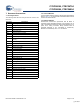
CY8C24094, CY8C24794 CY8C24894, CY8C24994 9. Register Reference This section lists the registers of the CY8C24x94 PSoC device family. For detailed register information, reference the PSoC Programmable System-on-Chip Technical Reference Manual. 9.1 Register Conventions 9.2 Register Mapping Tables The register conventions specific to this section are listed in the following table. The PSoC device has a total register address space of 512 bytes.
CY8C24094, CY8C24794 CY8C24894, CY8C24994 9.
CY8C24094, CY8C24794 CY8C24894, CY8C24994 9.
CY8C24094, CY8C24794 CY8C24894, CY8C24994 10. Electrical Specifications This section presents the DC and AC electrical specifications of the CY8C24x94 PSoC device family. For the most up to date electrical specifications, confirm that you have the most recent data sheet by going to the web at http://www.cypress.com/psoc. Specifications are valid for -40oC ≤ TA ≤ 85oC and TJ ≤ 100oC, except where noted. Specifications for devices running at greater than 12 MHz are valid for -40oC ≤ TA ≤ 70oC and TJ ≤ 82oC.
CY8C24094, CY8C24794 CY8C24894, CY8C24994 10.1 Absolute Maximum Ratings Table 10-2. Absolute Maximum Ratings Symbol Description TSTG Storage Temperature Min -55 Typ 25 Max +100 TA Vdd VI/O Ambient Temperature with Power Applied Supply Voltage on Vdd Relative to Vss DC Input Voltage – – – DC Voltage Applied to Tri-state IMI/O IMAI/O Maximum Current into any Port Pin Maximum Current into any Port Pin Configured as Analog Driver Electro Static Discharge Voltage Latch-up Current – – +85 +6.0 Vdd + 0.
CY8C24094, CY8C24794 CY8C24894, CY8C24994 10.3 DC Electrical Characteristics 10.3.1 DC Chip Level Specifications The following table lists guaranteed maximum and minimum specifications for the voltage and temperature ranges: 4.75V to 5.25V and -40°C ≤ TA ≤ 85°C, or 3.0V to 3.6V and -40°C ≤ TA ≤ 85°C, respectively. Typical parameters apply to 5V and 3.3V at 25°C and are for design guidance only. Table 10-4. DC Chip-Level Specifications Symbol Description Vdd Supply Voltage Min 3.0 – Typ Max 5.
CY8C24094, CY8C24794 CY8C24894, CY8C24994 10.3.3 DC Full-Speed USB Specifications The following table lists guaranteed maximum and minimum specifications for the voltage and temperature ranges: 4.75V to 5.25V and -10°C ≤ TA ≤ 85°C, or 3.0V to 3.6V and -10°C ≤ TA ≤ 85°C, respectively. Typical parameters apply to 5V and 3.3V at 25°C and are for design guidance only. Table 10-6.
CY8C24094, CY8C24794 CY8C24894, CY8C24994 Table 10-7. 5V DC Operational Amplifier Specifications (continued) Symbol VOHIGHO Description Min High Output Voltage Swing (internal signals) Vdd Power = Low, Opamp Bias = High A 0.2 Power = Medium, Opamp Bias = High Vdd Power = High, Opamp Bias = High 0.2 Vdd 0.
CY8C24094, CY8C24794 CY8C24894, CY8C24994 10.3.6 DC Analog Output Buffer Specifications The following tables list guaranteed maximum and minimum specifications for the voltage and temperature ranges: 4.75V to 5.25V and -40°C ≤ TA ≤ 85°C, or 3.0V to 3.6V and -40°C ≤ TA ≤ 85°C, respectively. Typical parameters apply to 5V and 3.3V at 25°C and are for design guidance only. Table 10-9.
CY8C24094, CY8C24794 CY8C24894, CY8C24994 10.3.7 DC Analog Reference Specifications The following tables list guaranteed maximum and minimum specifications for the voltage and temperature ranges: 4.75V to 5.25V and -40°C ≤ TA ≤ 85°C, or 3.0V to 3.6V and -40°C ≤ TA ≤ 85°C, respectively. Typical parameters apply to 5V and 3.3V at 25°C and are for design guidance only. The guaranteed specifications are measured through the Analog Continuous Time PSoC blocks.
CY8C24094, CY8C24794 CY8C24894, CY8C24994 Table 10-12. 3.3V DC Analog Reference Specifications (continued) Symbol – – – – – – Description RefHi = 3.2 x BandGap RefLo = Vdd/2 - BandGap RefLo = BandGap RefLo = 2 x BandGap - P2[6] (P2[6] = 0.5V) RefLo = P2[4] – BandGap (P2[4] = Vdd/2) RefLo = P2[4]-P2[6] (P2[4] = Vdd/2, P2[6] = 0.5V) Min Not Allowed Not Allowed Not Allowed Not Allowed Not Allowed P2[4] - P2[6] 0.048 Typ P2[4]- P2[6] + 0.022 Max Units P2[4] - P2[6] + 0.092 V 10.3.
CY8C24094, CY8C24794 CY8C24894, CY8C24994 10.3.9 DC POR and LVD Specifications The following table lists guaranteed maximum and minimum specifications for the voltage and temperature ranges: 4.75V to 5.25V and -40°C ≤ TA ≤ 85°C, or 3.0V to 3.6V and -40°C ≤ TA ≤ 85°C, respectively. Typical parameters apply to 5V or 3.3V at 25°C and are for design guidance only. Note The bits PORLEV and VM in the table below refer to bits in the VLT_CR register.
CY8C24094, CY8C24794 CY8C24894, CY8C24994 10.3.10 DC Programming Specifications The following table lists guaranteed maximum and minimum specifications for the voltage and temperature ranges: 4.75V to 5.25V and -40°C ≤ TA ≤ 85°C, or 3.0V to 3.6V and -40°C ≤ TA ≤ 85°C, respectively. Typical parameters apply to 5V and 3.3V at 25°C and are for design guidance only. Table 10-15.
CY8C24094, CY8C24794 CY8C24894, CY8C24994 10.4 AC Electrical Characteristics 10.4.1 AC Chip-Level Specifications The following table lists guaranteed maximum and minimum specifications for the voltage and temperature ranges: 4.75V to 5.25V and -40°C ≤ TA ≤ 85°C, or 3.0V to 3.6V and -40°C ≤ TA ≤ 85°C, respectively. Typical parameters apply to 5V and 3.3V at 25°C and are for design guidance only. Table 10-16.
CY8C24094, CY8C24794 CY8C24894, CY8C24994 10.0.1 AC General Purpose I/O Specifications The following table lists guaranteed maximum and minimum specifications for the voltage and temperature ranges: 4.75V to 5.25V and -40°C ≤ TA ≤ 85°C, or 3.0V to 3.6V and -40°C ≤ TA ≤ 85°C, respectively. Typical parameters apply to 5V and 3.3V at 25°C and are for design guidance only. Table 10-17.
CY8C24094, CY8C24794 CY8C24894, CY8C24994 10.0.2 AC Operational Amplifier Specifications The following tables list guaranteed maximum and minimum specifications for the voltage and temperature ranges: 4.75V to 5.25V and -40°C ≤ TA ≤ 85°C, or 3.0V to 3.6V and -40°C ≤ TA ≤ 85°C, respectively. Typical parameters apply to 5V and 3.3V at 25°C and are for design guidance only. Settling times, slew rates, and gain bandwidth are based on the Analog Continuous Time PSoC block.
CY8C24094, CY8C24794 CY8C24894, CY8C24994 When bypassed by a capacitor on P2[4], the noise of the analog ground signal distributed to each block is reduced by a factor of up to 5 (14 dB). This is at frequencies above the corner frequency defined by the on-chip 8.1k resistance and the external capacitor. Figure 10-4. Typical AGND Noise with P2[4] Bypass dBV/rtHz 10000 0 0.01 0.1 1.0 10 1000 100 0.001 0.01 0.
CY8C24094, CY8C24794 CY8C24894, CY8C24994 10.0.1 AC Low Power Comparator Specifications The following table lists guaranteed maximum and minimum specifications for the voltage and temperature ranges: 4.75V to 5.25V and -40°C ≤ TA ≤ 85°C, 3.0V to 3.6V and -40°C ≤ TA ≤ 85°C, or 2.4V to 3.0V and -40°C ≤ TA ≤ 85°C, respectively. Typical parameters apply to 5V at 25°C and are for design guidance only. Table 10-21.
CY8C24094, CY8C24794 CY8C24894, CY8C24994 10.0.3 AC External Clock Specifications The following tables list guaranteed maximum and minimum specifications for the voltage and temperature ranges: 4.75V to 5.25V and -40°C ≤ TA ≤ 85°C, or 3.0V to 3.6V and -40°C ≤ TA ≤ 85°C, respectively. Typical parameters apply to 5V and 3.3V at 25°C and are for design guidance only. Table 10-23. AC External Clock Specifications Symbol Description Min Typ Max Units FOSCEXT Frequency for USB Applications 23.94 24 24.
CY8C24094, CY8C24794 CY8C24894, CY8C24994 Table 10-25. 3.3V AC Analog Output Buffer Specifications Symbol Description TROB Rising Settling Time to 0.1%, 1V Step, 100 pF Load Power = Low Power = High TSOB Falling Settling Time to 0.
CY8C24094, CY8C24794 CY8C24894, CY8C24994 10.0.6 AC I2C Specifications The following table lists guaranteed maximum and minimum specifications for the voltage and temperature ranges: 4.75V to 5.25V and -40°C ≤ TA ≤ 85°C, or 3.0V to 3.6V and -40°C ≤ TA ≤ 85°C, respectively. Typical parameters apply to 5V and 3.3V at 25°C and are for design guidance only. Table 10-27.
CY8C24094, CY8C24794 CY8C24894, CY8C24994 11. Packaging Dimensions This section illustrates the package specification for the CY8C24x94 PSoC devices, along with the thermal impedance for the package and solder reflow peak temperatures. Important Note Emulation tools may require a larger area on the target PCB than the chip’s footprint. For a detailed description of the emulation tools’ dimensions, refer to the document titled PSoC Emulator Pod Dimensions at http://www.cypress.com/design/MR10161.
CY8C24094, CY8C24794 CY8C24894, CY8C24994 Figure 11-2. 68-Pin (8x8 mm x 0.89 mm) QFN 51-85214 *C Important Note ■ For information on the preferred dimensions for mounting QFN packages, see the following Application Note at http://www.amkor.com/products/notes_papers/MLFAppNote.pdf. ■ Pinned vias for thermal conduction are not required for the low-power PSoC device. Figure 11-3. 68-Pin SAWN QFN (8X8 mm X 0.90 mm) 001-09618 *A Document Number: 38-12018 Rev.
CY8C24094, CY8C24794 CY8C24894, CY8C24994 Figure 11-4. 100-Ball (6x6 mm) VFBGA 51-85209 *B Figure 11-5. 100-Pin (14x14 x 1.4 mm) TQFP 51-85048 *C Document Number: 38-12018 Rev.
CY8C24094, CY8C24794 CY8C24894, CY8C24994 11.1 Thermal Impedance Table 11-1. Thermal Impedance for the Package Typical θJA [15] Package 56 QFN[16] 12.93 oC/W 68 QFN[16] 13.05 oC/W 100 VFBGA 65 oC/W 100 TQFP 51 oC/W 11.2 Solder Reflow Peak Temperature Following is the minimum solder reflow peak temperature to achieve good solderability. Table 11-2.
CY8C24094, CY8C24794 CY8C24894, CY8C24994 12. Development Tool Selection 12.1 Software ■ iMAGEcraft C Compiler (Registration Required) 12.1.1 PSoC Designer™ ■ ISSP Cable At the core of the PSoC development software suite is PSoC Designer. Used by thousands of PSoC developers, this robust software has been facilitating PSoC designs for half a decade. PSoC Designer is available free of charge at http://www.cypress.com under DESIGN RESOURCES >> Software and Drivers. ■ USB 2.
CY8C24094, CY8C24794 CY8C24894, CY8C24994 12.3.2 CY3210-PSoCEval1 12.4 Device Programmers The CY3210-PSoCEval1 kit features an evaluation board and the MiniProg1 programming unit. The evaluation board includes an LCD module, potentiometer, LEDs, and plenty of breadboarding space to meet all of your evaluation needs. The kit includes: All device programmers can be purchased from the Cypress Online Store. 12.4.
CY8C24094, CY8C24794 CY8C24894, CY8C24994 13. Ordering Information XRES Pin Analog Outputs Analog Inputs Digital I/O Pins Analog Blocks Digital Blocks SRAM (Bytes) Temperature Range Flash (Bytes) Package Ordering Code Table 13-1.
CY8C24094, CY8C24794 CY8C24894, CY8C24994 13.1 Ordering Code Definitions CY 8 C 24 XXX- SP XX Package Type: PX = PDIP Pb-Free SX = SOIC Pb-Free PVX = SSOP Pb-Free LFX/LKX/LTX = QFN Pb-Free AX = TQFP Pb-Free BVX = VFBGA Pb-Free Speed: 24 MHz Thermal Rating: C = Commercial I = Industrial E = Extended Part Number Family Code Technology Code: C = CMOS Marketing Code: 8 = Cypress PSoC Company ID: CY = Cypress Note 21. This part may be used for in-circuit debugging. It is NOT available for production.
CY8C24094, CY8C24794 CY8C24894, CY8C24994 14. Document History Page Document Title: CY8C24094, CY8C24794, CY8C24894 and CY8C24994 PSoC® Programmable System-on-Chip™ Document Number: 38-12018 Rev. ECN No. Submission Date Orig. of Change Description of Change ** 133189 01.27.2004 NWJ New silicon and new document – Advance Data Sheet. *A 251672 See ECN SFV First Preliminary Data Sheet.
CY8C24094, CY8C24794 CY8C24894, CY8C24994 Sales, Solutions, and Legal Information Worldwide Sales and Design Support Cypress maintains a worldwide network of offices, solution centers, manufacturer’s representatives, and distributors. To find the office closest to you, visit us at cypress.com/sales. Products PSoC Clocks & Buffers PSoC Solutions psoc.cypress.com clocks.cypress.com General Low Power/Low Voltage psoc.cypress.com/solutions psoc.cypress.com/low-power Wireless wireless.cypress.