CY8C24123 CY8C24223, CY8C24423 PSoC® Programmable System-on-Chip™ Features ■ ■ ■ ■ ■ Powerful Harvard Architecture Processor ❐ M8C Processor Speeds to 24 MHz ❐ 8x8 Multiply, 32-Bit Accumulate ❐ Low Power at High Speed ❐ 3.0 to 5.25 V Operating Voltage ❐ Operating Voltages Down to 1.
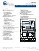
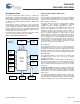
CY8C24123 CY8C24223, CY8C24423 PSoC® Functional Overview Digital System The PSoC® family consists of many Mixed Signal Array with On-Chip Controller devices. These devices are designed to replace multiple traditional MCU-based system components with one, low cost single-chip programmable device. PSoC devices include configurable blocks of analog and digital logic, and programmable interconnects.
CY8C24123 CY8C24223, CY8C24423 The Analog System is composed of six configurable blocks, each comprised of an opamp circuit allowing the creation of complex analog signal flows. Analog peripherals are very flexible and can be customized to support specific application requirements.
CY8C24123 CY8C24223, CY8C24423 Getting Started Additional System Resources System Resources, some of which have been previously listed, provide additional capability useful to complete systems. Additional resources include a multiplier, decimator, switch mode pump, low voltage detection, and power on reset. Brief statements describing the merits of each system resource follow: ■ ■ Digital clock dividers provide three customizable clock frequencies for use in applications.
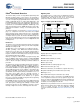
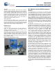
CY8C24123 CY8C24223, CY8C24423 Development Tools PSoC Designer Software Subsystems The Cypress MicroSystems PSoC Designer is a Microsoft® Windows-based, integrated development environment for the Programmable System-on-Chip (PSoC) devices. The PSoC Designer IDE and application runs on Windows 98, Windows NT 4.0, Windows 2000, Windows Millennium (Me), or Windows XP (refer Figure 3).
CY8C24123 CY8C24223, CY8C24423 Debugger The PSoC Designer Debugger subsystem provides hardware in-circuit emulation, allowing the designer to test the program in a physical system while providing an internal view of the PSoC device. Debugger commands allow the designer to read and program and read and write data memory, read and write IO registers, read and write CPU registers, set and clear breakpoints, and provide program run, halt, and step control.
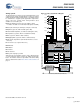
CY8C24123 CY8C24223, CY8C24423 Figure 5. User Module and Source Code Development Flows Acronyms Used Device Editor User Module Selection Placement and Parameter -ization Source Code Generator Application Editor Source Code Editor Build Manager Table 2.
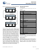
CY8C24123 CY8C24223, CY8C24423 Pinouts The CY8C24x23 PSoC device is available in a variety of packages which are listed and illustrated in the following tables. Every port pin (labeled with a “P”) is capable of Digital IO. However, Vss, Vdd, SMP, and XRES are not capable of Digital IO. 8-Pin Part Pinout Table 3. 8-Pin Part Pinout (PDIP, SOIC) Type Pin Pin No.
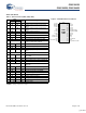
CY8C24123 CY8C24223, CY8C24423 28-Pin Part Pinout Table 5. 28-Pin Part Pinout (PDIP, SSOP, SOIC) Pin No. 1 2 3 4 5 6 7 8 9 10 11 12 13 14 15 16 17 18 19 20 21 22 23 24 25 26 27 28 Type Pin Description Digital Analog Name IO I P0[7] Analog column mux input IO IO P0[5] Analog column mux input and column output IO IO P0[3] Analog column mux input and column output IO I P0[1] Analog column mux input.
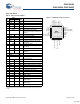
CY8C24123 CY8C24223, CY8C24423 32-Pin Part Pinout Table 6.
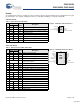
CY8C24123 CY8C24223, CY8C24423 Register Reference Register Mapping Tables This section lists the registers of the CY8C27xxx PSoC device by way of mapping tables, in offset order. For detailed register information, reference the PSoC Programmable System-on-Chip Technical Reference Manual. The PSoC device has a total register address space of 512 bytes. The register space is also referred to as IO space and is broken into two parts.
CY8C24123 CY8C24223, CY8C24423 Access Addr (0,Hex) Name Access Addr (0,Hex) Name Access Addr (0,Hex) Name Access Addr (0,Hex) Name Table 8.
CY8C24123 CY8C24223, CY8C24423 Access Addr (0,Hex) Name Access Addr (0,Hex) Name Access Addr (0,Hex) Name Access Addr (0,Hex) Name Table 8.
CY8C24123 CY8C24223, CY8C24423 ASC21CR3 97 RW Access Addr (1,Hex) Name Access Addr (1,Hex) Name Access Addr (1,Hex) Name Access Addr (1,Hex) Name Table 9.
CY8C24123 CY8C24223, CY8C24423 Electrical Specifications This section presents the DC and AC electrical specifications of the CY8C24x23 PSoC device. For latest electrical specifications, http://www.cypress.com. Specifications are valid for -40oC ≤ TA ≤ 85oC and TJ ≤ 100oC, except where noted. Specifications for devices running at greater than 12 MHz are valid for -40oC ≤ TA ≤ 70oC and TJ ≤ 82oC. Figure 10. Voltage versus Operating Frequency 5.25 Vdd Voltage lid ng Va rati n pe io O Reg 4.75 3.
CY8C24123 CY8C24223, CY8C24423 Absolute Maximum Ratings Exceeding maximum ratings may shorten the useful life of the device. User guidelines are not tested. Table 11. Absolute Maximum Ratings Symbol Description TSTG Storage Temperature TA Vdd VIO – IMIO IMAIO – – Min -55 Ambient Temperature with Power Applied -40 Supply Voltage on Vdd Relative to Vss -0.5 DC Input Voltage Vss - 0.5 DC Voltage Applied to Tri-state Vss - 0.
CY8C24123 CY8C24223, CY8C24423 DC Electrical Characteristics DC Chip-Level Specifications The following table lists guaranteed maximum and minimum specifications for the voltage and temperature ranges: 4.75V to 5.25V and -40°C ≤ TA ≤ 85°C, or 3.0V to 3.6V and -40°C ≤ TA ≤ 85°C, respectively. Typical parameters apply to 5V and 3.3V at 25°C and are for design guidance only or unless otherwise specified. Table 13. DC Chip-Level Specifications Symbol Description Vdd Supply Voltage IDD Supply Current Min 3.
CY8C24123 CY8C24223, CY8C24423 DC General Purpose IO Specifications The following table lists guaranteed maximum and minimum specifications for the voltage and temperature ranges: 4.75V to 5.25V and -40°C ≤ TA ≤ 85°C, or 3.0V to 3.6V and -40°C ≤ TA ≤ 85°C, respectively. Typical parameters apply to 5V and 3.3V at 25°C and are for design guidance only or unless otherwise specified. Table 14.
CY8C24123 CY8C24223, CY8C24423 Table 15. 5V DC Operational Amplifier Specifications (continued) Symbol GOLOA Description Open Loop Gain Power = Low Power = Medium Power = High Min Max – – – – – – – V V V – – – 0.2 0.2 0.5 V V V 150 300 600 1200 2400 4600 – 200 400 800 1600 3200 6400 – μA μA μA μA μA μA dB 60 60 80 VOHIGHOA High Output Voltage Swing (worst case internal load) Vdd - 0.2 Power = Low Vdd - 0.2 Power = Medium Vdd - 0.
CY8C24123 CY8C24223, CY8C24423 Table 16. 3.3V DC Operational Amplifier Specifications Symbol Min Typ Max Units – – 1.65 1.32 10 8 mV mV TCVOSOA Average Input Offset Voltage Drift – 7.0 35.0 μV/oC IEBOA Input Leakage Current (Port 0 Analog Pins) – 20 – pA Gross tested to 1 μA. CINOA Input Capacitance (Port 0 Analog Pins) – 4.5 9.5 pF Package and pin dependent. Temp = 25oC. VCMOA Common Mode Voltage Range 0.2 – Vdd - 0.
CY8C24123 CY8C24223, CY8C24423 DC Analog Output Buffer Specifications The following tables list guaranteed maximum and minimum specifications for the voltage and temperature ranges: 4.75V to 5.25V and -40°C ≤ TA ≤ 85°C, or 3.0V to 3.6V and -40°C ≤ TA ≤ 85°C, respectively. Typical parameters apply to 5V and 3.3V at 25°C and are for design guidance only or unless otherwise specified. Table 17.
CY8C24123 CY8C24223, CY8C24423 DC Switch Mode Pump Specifications The following table lists guaranteed maximum and minimum specifications for the voltage and temperature ranges: 4.75V to 5.25V and -40°C ≤ TA ≤ 85°C, or 3.0V to 3.6V and -40°C ≤ TA ≤ 85°C, respectively. Typical parameters apply to 5V and 3.3V at 25°C and are for design guidance only or unless otherwise specified. Table 19.
CY8C24123 CY8C24223, CY8C24423 DC Analog Reference Specifications The following tables list guaranteed maximum and minimum specifications for the voltage and temperature ranges: 4.75V to 5.25V and -40°C ≤ TA ≤ 85°C, or 3.0V to 3.6V and -40°C ≤ TA ≤ 85°C, respectively. Typical parameters apply to 5V and 3.3V at 25°C and are for design guidance only or unless otherwise specified. The guaranteed specifications are measured through the Analog Continuous Time PSoC blocks.
CY8C24123 CY8C24223, CY8C24423 Table 21. 3.3V DC Analog Reference Specifications Symbol Description BG Bandgap Voltage Reference – AGND = Vdd/2a CT Block Power = High – AGND = 2 x BandGapa CT Block Power = High – AGND = P2[4] (P2[4] = Vdd/2) CT Block Power = High – AGND = BandGapa CT Block Power = High – AGND = 1.
CY8C24123 CY8C24223, CY8C24423 DC Analog PSoC Block Specifications The following table lists guaranteed maximum and minimum specifications for the voltage and temperature ranges: 4.75V to 5.25V and -40°C ≤ TA ≤ 85°C, or 3.0V to 3.6V and -40°C ≤ TA ≤ 85°C, respectively. Typical parameters apply to 5V and 3.3V at 25°C and are for design guidance only or unless otherwise specified. Table 22.
CY8C24123 CY8C24223, CY8C24423 DC Programming Specifications The following table lists guaranteed maximum and minimum specifications for the voltage and temperature ranges: 4.75V to 5.25V and -40°C ≤ TA ≤ 85°C, or 3.0V to 3.6V and -40°C ≤ TA ≤ 85°C, respectively. Typical parameters apply to 5V and 3.3V at 25°C and are for design guidance only or unless otherwise specified. Table 24.
CY8C24123 CY8C24223, CY8C24423 AC Electrical Characteristics AC Chip-Level Specifications The following table lists guaranteed maximum and minimum specifications for the voltage and temperature ranges: 4.75V to 5.25V and -40°C ≤ TA ≤ 85°C, or 3.0V to 3.6V and -40°C ≤ TA ≤ 85°C, respectively. Typical parameters apply to 5V and 3.3V at 25°C and are for design guidance only or unless otherwise specified. Table 25.
CY8C24123 CY8C24223, CY8C24423 Figure 12. PLL Lock Timing Diagram PLL Enable TPLLSLEW 24 MHz FPLL PLL Gain 0 Figure 13. PLL Lock for Low Gain Setting Timing Diagram PLL Enable TPLLSLEWLOW 24 MHz FPLL PLL Gain 1 Figure 14. External Crystal Oscillator Startup Timing Diagram 32K Select 32 kHz TOS F32K2 Figure 15. 24 MHz Period Jitter (IMO) Timing Diagram Jitter24M1 F24M Figure 16. 32 kHz Period Jitter (ECO) Timing Diagram Jitter32k F32K2 Document Number: 38-12011 Rev.
CY8C24123 CY8C24223, CY8C24423 AC General Purpose IO Specifications The following table lists guaranteed maximum and minimum specifications for the voltage and temperature ranges: 4.75V to 5.25V and -40°C ≤ TA ≤ 85°C, or 3.0V to 3.6V and -40°C ≤ TA ≤ 85°C, respectively. Typical parameters apply to 5V and 3.3V at 25°C and are for design guidance only or unless otherwise specified. Table 26.
CY8C24123 CY8C24223, CY8C24423 AC Operational Amplifier Specifications The following tables list guaranteed maximum and minimum specifications for the voltage and temperature ranges: 4.75V to 5.25V and -40°C ≤ TA ≤ 85°C, or 3.0V to 3.6V and -40°C ≤ TA ≤ 85°C, respectively. Typical parameters apply to 5V and 3.3V at 25°C and are for design guidance only or unless otherwise specified. Note Settling times, slew rates, and gain bandwidth are based on the Analog Continuous Time PSoC block. Table 27.
CY8C24123 CY8C24223, CY8C24423 Table 28. 3.3V AC Operational Amplifier Specifications Symbol TROA TSOA SRROA SRFOA BWOA ENOA Description Rising Settling Time from 80% of ΔV to 0.1% of ΔV (10 pF load, Unity Gain) Power = Low Power = Low, Opamp Bias = High Power = Medium Power = Medium, Opamp Bias = High Power = High (3.3 Volt High Bias Operation not supported) Power = High, Opamp Bias = High (3.3 Volt High Power, High Opamp Bias not supported) Falling Settling Time from 20% of ΔV to 0.
CY8C24123 CY8C24223, CY8C24423 AC Digital Block Specifications The following table lists guaranteed maximum and minimum specifications for the voltage and temperature ranges: 4.75V to 5.25V and -40°C ≤ TA ≤ 85°C, or 3.0V to 3.6V and -40°C ≤ TA ≤ 85°C, respectively. Typical parameters apply to 5V and 3.3V at 25°C and are for design guidance only or unless otherwise specified. Table 29.
CY8C24123 CY8C24223, CY8C24423 AC Analog Output Buffer Specifications The following tables list guaranteed maximum and minimum specifications for the voltage and temperature ranges: 4.75V to 5.25V and -40°C ≤ TA ≤ 85°C, or 3.0V to 3.6V and -40°C ≤ TA ≤ 85°C, respectively. Typical parameters apply to 5V and 3.3V at 25°C and are for design guidance only or unless otherwise specified. Table 30.
CY8C24123 CY8C24223, CY8C24423 AC External Clock Specifications The following tables list guaranteed maximum and minimum specifications for the voltage and temperature ranges: 4.75V to 5.25V and -40°C ≤ TA ≤ 85°C, or 3.0V to 3.6V and -40°C ≤ TA ≤ 85°C, respectively. Typical parameters apply to 5V and 3.3V at 25°C and are for design guidance only or unless otherwise specified. Table 32. 5V AC External Clock Specifications Symbol Description Min Typ Max Units FOSCEXT Frequency 0 – 24.
CY8C24123 CY8C24223, CY8C24423 AC I2C Specifications The following table lists guaranteed maximum and minimum specifications for the voltage and temperature ranges: 4.75V to 5.25V and -40°C ≤ TA ≤ 85°C, or 3.0V to 3.6V and -40°C ≤ TA ≤ 85°C, respectively. Typical parameters apply to 5V and 3.3V at 25°C and are for design guidance only or unless otherwise specified. Table 35.
CY8C24123 CY8C24223, CY8C24423 Packaging Information This section presents the packaging specifications for the CY8C24x23 PSoC device, along with the thermal impedances for each package and the typical package capacitance on crystal pins. Figure 19. 8-Pin (300-Mil) PDIP 51-85075 *A Document Number: 38-12011 Rev.
CY8C24123 CY8C24223, CY8C24423 Figure 20. 8-Pin (150-Mil) SOIC 51-85066 *B 51-85066 *C Figure 21. 20-Pin (300-Mil) Molded DIP ( ) 51-85011-A 51-85011 *A Document Number: 38-12011 Rev.
CY8C24123 CY8C24223, CY8C24423 Figure 22. 20-Pin (210-Mil) SSOP 51-85077 *C Figure 23. 20-Pin (300-Mil) Molded SOIC 51-85024 *C Document Number: 38-12011 Rev.
CY8C24123 CY8C24223, CY8C24423 Figure 24. 28-Pin (300-Mil) Molded DIP 51-85014 *D Document Number: 38-12011 Rev.
CY8C24123 CY8C24223, CY8C24423 Figure 25. 28-Pin (210-Mil) SSOP 51-85079 *C Figure 26. 28-Pin (300-Mil) Molded SOIC 51-85026 *D Document Number: 38-12011 Rev.
CY8C24123 CY8C24223, CY8C24423 Figure 27. 32-Pin (5x5 mm) MLF 51-85188 *B Thermal Impedances Capacitance on Crystal Pins Table 36. Thermal Impedances per Package Table 37. Typical Package Capacitance on Crystal Pins Package Typical θJA * Package Package Capacitance 8 PDIP 123 oC/W 8 PDIP 2.8 pF 8 SOIC 185 oC/W 8 SOIC 2.0 pF 20 PDIP 109 oC/W 20 PDIP 3.0 pF 20 SSOP o 117 C/W 20 SSOP 2.6 pF 20 SOIC 81 oC/W 20 SOIC 2.5 pF 28 PDIP 69 oC/W 28 SSOP 101 oC/W 28 PDIP 3.
CY8C24123 CY8C24223, CY8C24423 Ordering Information The following table lists the CY8C24x23 PSoC Device family’s key package features and ordering codes.
CY8C24123 CY8C24223, CY8C24423 Document History Page Document Title: CY8C24123, CY8C24223, CY8C24423 PSoC® Programmable System-on-Chip™ Document Number: 38-12011 ECN Orig. of Change ** 127043 New Silicon and NWJ 05/15/2003 New document – Advanced Data Sheet (two page product brief). *A 128779 NWJ 08/13/2003 New document – Preliminary Data Sheet (300 page product detail).